

Conductive member, method for producing conductive member, touch panel, and solar cell
A technology for conductive components and manufacturing methods, which can be applied to conductive materials dispersed in non-conductive inorganic materials, printed circuit manufacturing, cable/conductor manufacturing, etc. problem, to achieve the effect of high tolerance, excellent electrical conductivity, and excellent flexibility
- Summary
- Abstract
- Description
- Claims
- Application Information
AI Technical Summary
Problems solved by technology
Method used
Image

Examples
example
[0384] Hereinafter, examples of the present invention will be described, but the present invention is not limited by these examples. In addition, "%" and "part" which are content in an example are based on a mass standard.
[0385] In the following examples, the average diameter (average minor axis length) and average major axis length of metal nanowires, the coefficient of variation of minor axis length, and the ratio of silver nanowires with an aspect ratio of 10 or more were measured as follows.
[0386]
[0387] Diameter (minor axis length) and major axis length of 300 randomly selected metal nanowires from among metal nanowires subjected to enlarged observation with a transmission electron microscope (TEM; manufactured by JEOL Ltd., JEM-2000FX) The measurement was performed, and the average diameter (average minor axis length) and the average major axis length of the metal nanowires were obtained from the average values.
[0388]
[0389] The short-axis length (diame...
Synthetic example 1
[0408]
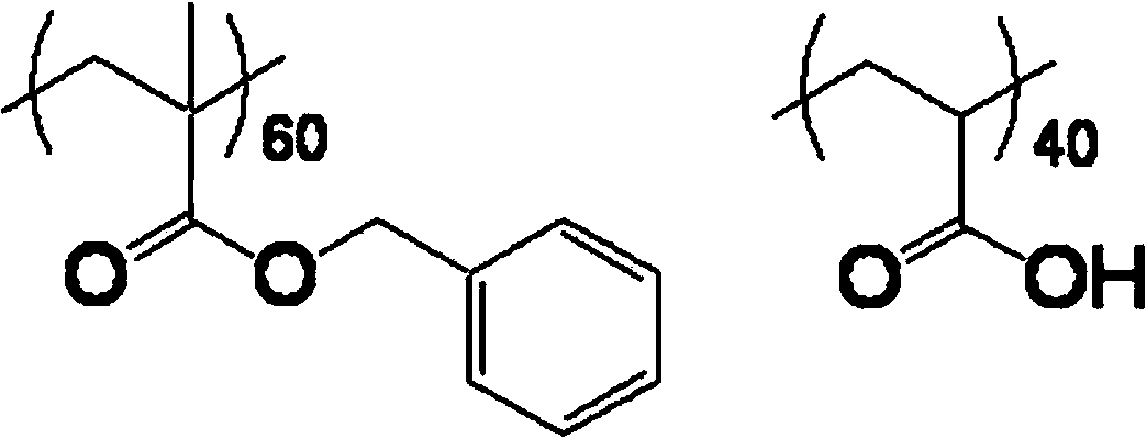
[0409] Use AA (9.64g), BzMA (35.36g) as the monomer component that constitutes copolymer, use AIBN (0.5g) as radical polymerization initiator, make these carry out polymerization reaction in solvent PGMEA (55.00g), borrow This obtained a PGMEA solution (solid content concentration: 45% by mass) of the binder (A-1). Furthermore, the polymerization temperature is adjusted to a temperature of 60°C to 100°C.
[0410] As a result of measuring the molecular weight by gel permeation chromatography (GPC), the polystyrene-equivalent weight average molecular weight (Mw) was 11000, the molecular weight distribution (Mw / Mn) was 1.72, and the acid value was 155 mgKOH / g.
[0411] [Chem 2]
[0412]
[0413] Adhesive (A-1)
Synthetic example 2
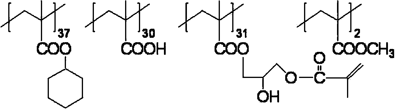
[0415]
[0416] 7.48 g of MFG (manufactured by Nippon Emulsifier Co., Ltd.) was added to the reaction vessel in advance, and the temperature was raised to 90° C., and then MAA (14.65 g), MMA (0.54 g), CHMA (17.55g), AIBN (0.50g) and the mixed solution of MFG (55.2g) which are radical polymerization initiators were dripped at 90 degreeC reaction container. After the dropwise addition, it was reacted for 4 hours to obtain an acrylic resin solution.
[0417] Then, after adding hydroquinone monomethyl ether 0.15g and tetraethylammonium bromide 0.34g to the obtained acrylic resin solution, GMA12.26g was dripped over 2 hours. After the dropwise addition, it was reacted at 90° C. for 4 hours while blowing air, and then prepared by adding PGMEA so that the solid content concentration became 45%, thereby obtaining a solution of the binder (A-2) (solid content Concentration: 45%).
[0418] As a result of measuring the molecular weight by gel permeation chromatography (GPC), the poly...
PUM
| Property | Measurement | Unit |
|---|---|---|
| length | aaaaa | aaaaa |
| length | aaaaa | aaaaa |
| length | aaaaa | aaaaa |
Abstract
Description
Claims
Application Information