Gas sensor based on field effect transistor structure and preparation method thereof
A field-effect transistor and gas sensor technology, which is applied in the field of field-effect transistor-based gas sensor and its preparation, can solve the problems of complex devices, high sensor cost, and long operation time, and achieve reduced volume and cost, and detection range The effect of wide and good application prospects
- Summary
- Abstract
- Description
- Claims
- Application Information
AI Technical Summary
Problems solved by technology
Method used
Image

Examples
Embodiment 1
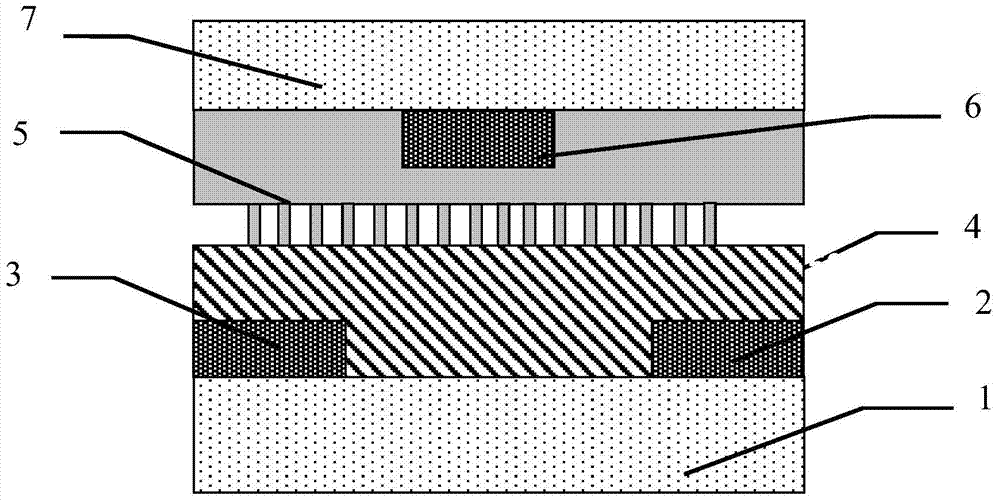
[0042] The gas sensor obtained in this embodiment is based on the top grid-bottom contact type, and its preparation method is as follows:
[0043] (1) On the base layer A1, use thermal evaporation to prepare a layer of gold material with a thickness of 100nm and a mirror-symmetrical source electrode 2 and drain electrode 3. The width of the source and drain electrodes is 200 μm, and the length is 200 μm. The distance is 20μm;
[0044] (2) On the base layer A1, the source electrode 2 and the drain electrode 3, phthalocyanine copper with a thickness of 80 nm is evaporated by thermal evaporation as the active layer 4;
[0045] (3) Prepare a layer of 100nm-thick gate electrode 6 on the base layer B7 by sputtering. The water was sonicated for 40 minutes, followed by N 2 Blow dry, place in a vacuum oven at 100°C for 10 minutes to obtain the base layer;
[0046] (4) On the base layer B7 and the gate electrode 6, prepare a PMMA layer by spin coating;
[0047] (5) On the surface of...
Embodiment 2
[0055] The gas sensor prepared in this example is based on the top grid-bottom contact type, and its preparation method is as follows:
[0056] (1) On the base layer A1, prepare a mirror-symmetric gold source electrode 2 and drain electrode 3 with a thickness of 100 nm by sputtering. The source and drain electrodes have a width of 200 μm and a length of 200 μm. The distance between them is 20 μm;
[0057] (2) transfer the single crystal of tetracene to the layer A1, the source electrode 2 and the drain electrode 3 as the active layer 4 by using the transfer method;
[0058] (3) Prepare a 60nm-thick gate electrode 6 on the base layer B7 by sputtering, and the gate electrode is made of gold; wherein, the base layer is prepared by using silicon as the base, followed by acetone, ethanol, pure The water was sonicated for 40 minutes, followed by N 2 Blow dry, place in a vacuum oven at 100°C for 10 minutes to obtain the base layer;
[0059] (4) On the base layer B7 and the gate el...
Embodiment 3
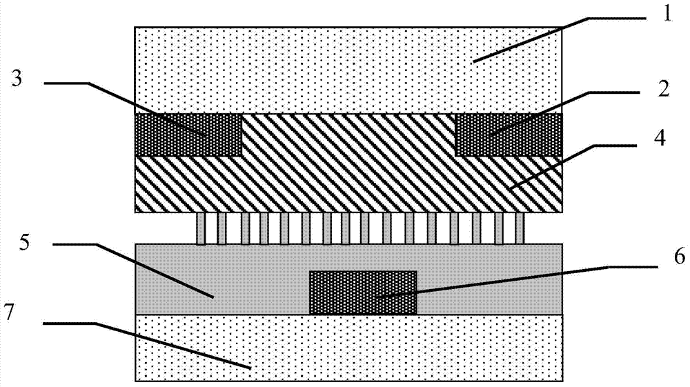
[0064] The gas sensor prepared in this example is based on the bottom gate-top contact type, and its preparation method is as follows:
[0065] (1) Prepare a mirror-symmetrical source electrode 2 and drain electrode 3 made of silver with a thickness of 300 nm on the base layer A1 by inkjet printing; the source and drain electrodes have a width of 200 μm and a length of 200 μm, The distance between the two electrodes is 50 μm;
[0066] (2) On the source electrode 2 and the drain electrode 3, a layer of vanadyl phthalocyanine with a thickness of 80 nanometers is prepared as the active layer 4 by thermal evaporation;
[0067] (3) Prepare a 60nm-thick gate electrode 6 on the base layer B7 by sputtering, and the gate electrode is made of gold; wherein, the base layer is prepared by using silicon as the base, followed by acetone, ethanol, pure The water was sonicated for 40 minutes, followed by N 2 Blow dry, place in a vacuum oven at 100°C for 10 minutes to obtain the base layer; ...
PUM
| Property | Measurement | Unit |
|---|---|---|
| Height | aaaaa | aaaaa |
| Diameter | aaaaa | aaaaa |
| Diameter | aaaaa | aaaaa |
Abstract
Description
Claims
Application Information
PatSnap Eureka turns technology decisions into work you can execute. Powered by our Innovation Knowledge Graph, it runs expert workflows across engineering, life sciences, materials and intellectual property. Get your review-ready output in minutes.


