
High-sensitivity hot electron thermal radiation detection meter and producing method thereof

A thermal radiation and detector technology, applied in electrical radiation detectors, circuits, electrical components, etc., can solve the problems of inability to achieve multi-layer structure absorption rate, affecting device response speed, serious device heat leakage, etc. The effect of small external interference and low cost

Active Publication Date: 2014-01-29
PEKING UNIV
View PDF4 Cites 3 Cited by
  • Summary
  • Abstract
  • Description
  • Claims
  • Application Information

AI Technical Summary

Problems solved by technology

In this way, although the response rate can reach 2×10 5 V / W, but the device preparation process of the double-layer graphene double-gate structure is quite complicated, and the heat leakage of the device is also serious
At the same time, the resistance of the device is relatively large, which affects the response speed of the device.
Since single-layer graphene is very thin, the absorption rate of light is only 2.3%. Thermionic radiation detectors based on graphene face the problem of low absorption efficiency. The above structures cannot achieve multi-layer structures to increase the absorption rate.

Method used


Image

  • High-sensitivity hot electron thermal radiation detection meter and producing method thereof
  • High-sensitivity hot electron thermal radiation detection meter and producing method thereof
  • High-sensitivity hot electron thermal radiation detection meter and producing method thereof

Examples


Embodiment 1

[0042] Embodiment 1, preparation of disordered graphene electronic thermal radiation detector

[0043] 1) Using SiO 2 285nm thick SiO 2 / N-Si substrate, which was purchased from the Institute of Microelectronics, Peking University. SiO with acetone 2 / N-Si substrates were ultrasonically cleaned to remove organic residues, and then they were ultrasonically cleaned with deionized water to remove impurities such as metal ions, and then the samples were quickly dried with a nitrogen gun.

[0044] 2) Throw a layer of PMMA with a molecular weight of 950K, a mass fraction of 6%, and a thickness of about 300nm at a speed of 3000r / min for 45 seconds (the start and stop time is 15 seconds), and bake at 170°C for 4 minutes.

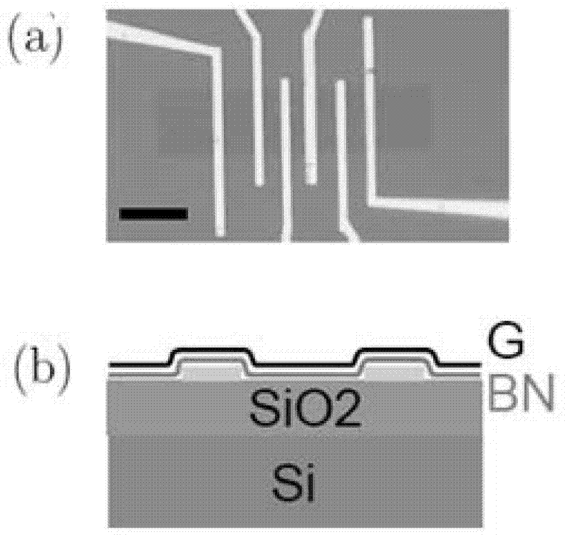
[0045] 2) Electron beam exposure is carried out on the substrate after gluing at the selected position to produce such as figure 1 The six-electrode structure with a spacing of 2.5 μm in (a).

[0046] The electron beam exposure machine used in this experiment i...


PUM


Abstract

The invention discloses an electron thermal radiation detection meter and a producing method thereof. The method includes 1, coating on an SiO2 liner to obtain a PMMA layer; performing electron beam exposure and development on the PMMA layer sequentially to obtain an electrode pattern, and then evaporating an electrode; 2, removing the PMMA layer from the SiO2 liner; transferring a boron nitride-disordered grapheme film, namely a composite film formed by sequentially stacking a boron nitride film and a disordered grapheme film, on the SiO2 liner; arranging the disordered grapheme film on the end face of the SiO2 liner with the evaporated electrode; 3, coating on the boron nitride-disordered grapheme film to obtain a PMMA layer, then obtaining a structure corresponding to the electrode through electron beam exposure and etching sequentially, and obtaining the electron thermal radiation detection meter. Compared with an existing grapheme thermal radiation detection meter produced by using superconducting tunnel junctions, the electron thermal radiation detection meter can operate without extreme low temperature but with an ordinary liquid helium refrigerator, cost is reduced, and operation is very simple.

Description

technical field [0001] The invention relates to a high-sensitivity thermal electron thermal radiation detector and a preparation method thereof. Background technique [0002] As a new type of two-dimensional material, graphene has high carrier mobility and good electrical, optical, thermal, mechanical and other properties, making it more and more widely used in various devices in recent years. Graphene has a unique Dirac electronic band structure, and the density of states near the Dirac point is close to zero, so that graphene has a small electronic heat capacity. In addition, graphene itself has weak electron-phonon coupling at room temperature and good thermal response to light radiation in different wavelength bands, which has made everyone wonder how to achieve high sensitivity and high response speed thermal energy from graphene in recent years. Research on radiation detectors is gaining more and more attention. [0003] At present, there are many ways to realize the...

Claims


Application Information

Patent Timeline
IPC IPC(8): G01J5/20
CPCH01L31/09
Inventor 吴孝松韩琪
Owner PEKING UNIV
Learn More