Method and corresponding device for restraining tunneling transistor from leaking current and method for manufacturing corresponding device

A technology of tunneling transistors and tunneling junctions, applied in semiconductor/solid-state device manufacturing, semiconductor devices, electrical components, etc., can solve TFET device leakage current and subthreshold slope degradation, limit the application of TFET devices, and increase device process complexity and other problems, to achieve the effect of suppressing self-heating effect, suppressing tunneling current, and reducing the probability of band-to-band tunneling

Active Publication Date: 2014-02-05
PEKING UNIV
View PDF5 Cites 4 Cited by
  • Summary
  • Abstract
  • Description
  • Claims
  • Application Information

AI Technical Summary

Problems solved by technology

TFET has many excellent characteristics such as low leakage current, low subthreshold slope, low operating voltage, and low power consumption. Limit the application of TFET devices
On the other hand, for small-sized TFETs, when the gate length is less than about 20nm, the direct band-band tunneling current from source to drain in the body region will increase sharply, which will seriously degrade the leakage current and subthreshold slope of the TFET device.
TFETs using ultra-thin body SOI substrates can suppress this short-channel effect to a certain extent, but due to the existence of the buried oxide layer under the thin silicon film, the heat dissipation problem will become the main problem, and the self-heating effect is serious, which affects the device characteristics. Film requirements also increase the process complexity of the device

Method used


Image

  • Method and corresponding device for restraining tunneling transistor from leaking current and method for manufacturing corresponding device
  • Method and corresponding device for restraining tunneling transistor from leaking current and method for manufacturing corresponding device
  • Method and corresponding device for restraining tunneling transistor from leaking current and method for manufacturing corresponding device

Examples


Embodiment Construction

[0045] The present invention will be further described below by example. It should be noted that the purpose of the disclosed embodiments is to help further understand the present invention, but those skilled in the art can understand that various replacements and modifications are possible without departing from the spirit and scope of the present invention and the appended claims of. Therefore, the present invention should not be limited to the content disclosed in the embodiments, and the protection scope of the present invention is subject to the scope defined in the claims.

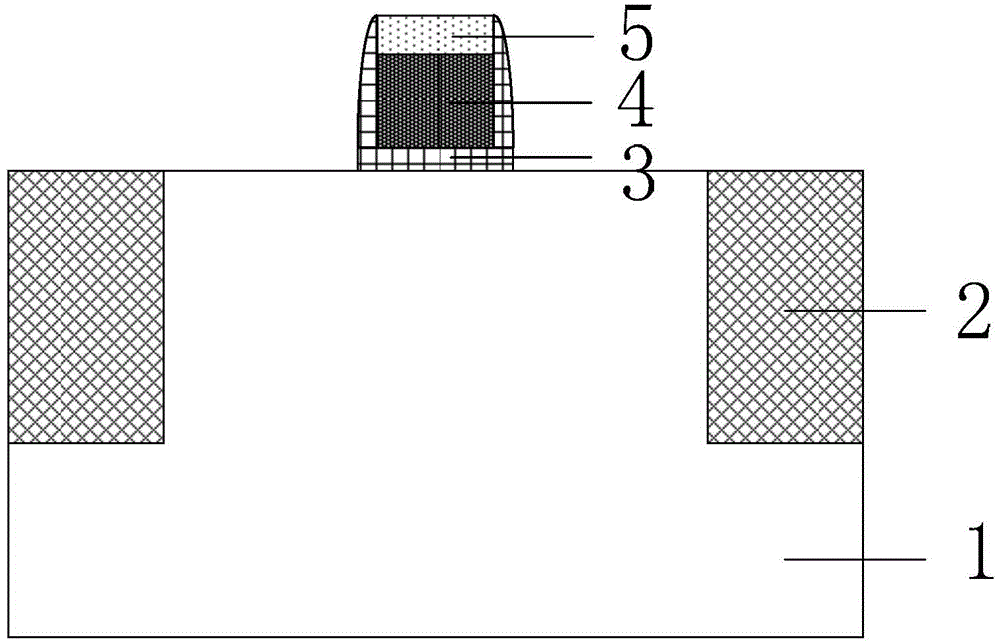
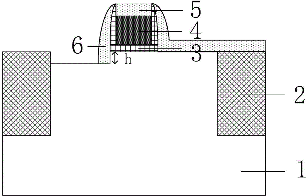
[0046] A specific example of the preparation method of the present invention includes Figure 1 to Figure 8 Process steps shown:

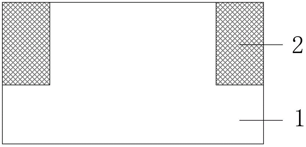
[0047] 1. Select a bulk silicon wafer silicon substrate 1 with a crystal orientation of (100) to make an active region isolation layer 2 using shallow trench isolation technology, and the doping concentration of the substrate is lightly doped, such as figure 1 shown. ...


PUM


Abstract

The invention discloses a method and corresponding device for restraining a tunneling transistor from leaking a current and a method for manufacturing the corresponding device and belongs to the field of field effect transistors and currents in a ULSI of a CMOS. According to the method for restraining the tunneling transistor from leaking the current, an insulating layer is inserted between a source zone and a body zone below a tunnel junction, an insulating layer is not inserted in the portion, between the source zone and a tunnel, of the tunnel junction, so that the source zone and a drain zone in a small-size TFET device are effectively prevented from being directly tunneled and leaking the current, and meanwhile the slope of a subthreshold value can be effectively improved. The method for manufacturing the corresponding device is compatible with the existing CMOS technology.

Description

technical field [0001] The invention belongs to the field of field effect transistor logic devices and circuits in CMOS ultra large integrated circuits (ULSI), and in particular relates to a method for suppressing the leakage current of tunneling transistors, a corresponding device and a preparation method. Background technique [0002] Driven by Moore's Law, the feature size of traditional MOSFETs has been shrinking, and now it has entered the nanometer scale. As a result, the negative effects of short-channel effects on devices have become more serious. The leakage-induced barrier reduction, band-band tunneling and other effects make the off-state leakage current of the device continuously increase. At the same time, the sub-threshold slope of the traditional MOSFET is limited by the thermoelectric potential and cannot be reduced synchronously with the shrinking of the device size, thus increasing device power consumption. The power consumption problem has become the most...

Claims


Application Information

Patent Timeline
Patent Type & Authority Applications(China)
IPC IPC(8): H01L29/06H01L29/36H01L21/336H01L29/417
CPCH01L29/36H01L29/66356H01L29/7391H01L29/0653H01L29/0834H01L21/02238H01L21/26513H01L21/266H01L21/308H01L21/32139H01L29/0638H01L29/0649H01L29/0847H01L29/1033H01L29/66659H01L29/7835
Inventor 黄如黄芊芊吴春蕾王佳鑫王超王阳元
Owner PEKING UNIV
Why Eureka
Try Eureka