Method for growing high-quality all-component adjustable ternary semiconductor alloy

A semiconductor, all-component technology, used in semiconductor devices, semiconductor/solid-state device manufacturing, electrical components, etc., can solve the problem of low crystal quality, and achieve high electron mobility, strong band-edge luminescence, and low background electron concentration. Effect

Inactive Publication Date: 2014-02-12
PEKING UNIV
View PDF2 Cites 2 Cited by
  • Summary
  • Abstract
  • Description
  • Claims
  • Application Information

AI Technical Summary

Problems solved by technology

[0004] In the current method of growing III-V ternary semiconductor alloys, ternary semiconductor alloys with different components are mainly grown by controlling the atomic beam ratio of each metal, but there is no systematic study on how the optimal growth temperature depends on the alloy composition , resulting in poor crystal quality

Method used


Image

  • Method for growing high-quality all-component adjustable ternary semiconductor alloy
  • Method for growing high-quality all-component adjustable ternary semiconductor alloy
  • Method for growing high-quality all-component adjustable ternary semiconductor alloy

Examples


Embodiment 1

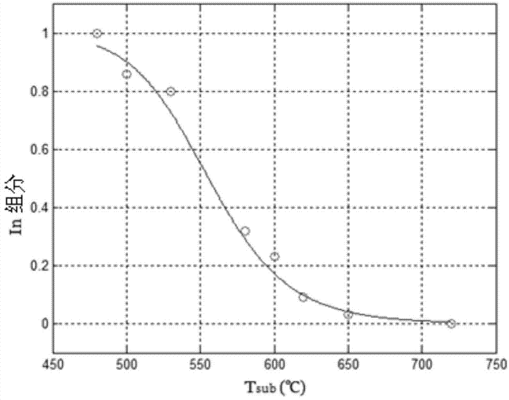
[0035] In this example, five pieces of high-quality In x Ga 1-x N alloy, In components are 0.1, 0.3, 0.5, 0.7, 0.9 respectively. The MBE method is used to grow on the GaN template. The growth process is carried out in an ultra-high vacuum growth chamber. The high-purity (7N) metal source is generated by a K-Cell source furnace. The nitrogen source is a radio frequency plasma nitrogen source. The growth process uses reflected high-energy electrons. In situ monitoring by diffractometer RHEED.

[0036] The preparation method of the full-component adjustable ternary semiconductor alloy in this embodiment includes the following steps:

[0037] 1) Pre-treat the template to make the surface of the template clean:

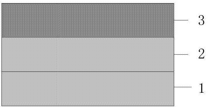
[0038] Raise the temperature of the GaN template 1 to about 600°C, bake for 10-30 minutes, then raise the temperature of the GaN template to about 800°C, and grow a layer of GaN material 2 with a thickness of 50-100nm, such as figure 1 shown;

[0039] 2) Determine the...

Embodiment 2

[0051] In this embodiment, growth of In lattice-matched with GaN 0.18 Al 0.82 N alloy. The MBE method is used to grow on the GaN template. The growth process is carried out in an ultra-high vacuum growth chamber. The high-purity (7N) metal source is generated by a K-Cell source furnace. The nitrogen source uses a radio frequency plasma nitrogen source, and the growth process uses reflective high-energy electrons. In situ monitoring by diffractometer RHEED.

[0052] The preparation method of the full-component adjustable ternary semiconductor alloy in this embodiment includes the following steps:

[0053] 1) Pre-treat the template to make the surface of the template clean:

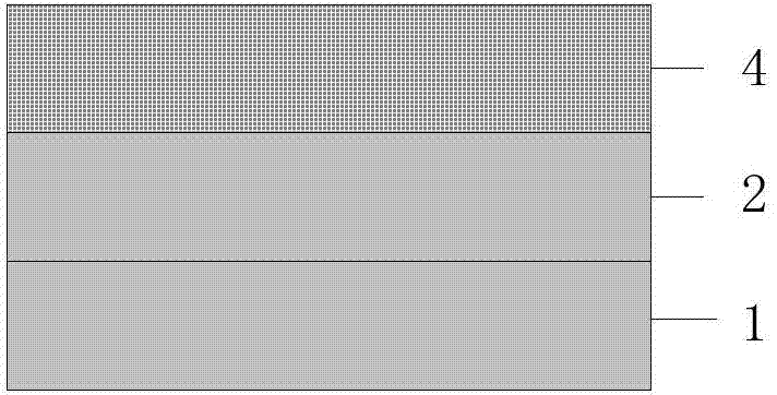
[0054] Raise the temperature of the GaN template 1 to about 600°C, bake for 10-30 minutes, then raise the temperature of the GaN template to about 800°C, and grow a layer of GaN material 2 with a thickness of 50-100nm, such as image 3 shown;

[0055] 2) Determine the composition In of each atom of the...


PUM

PropertyMeasurementUnit
Surface roughnessaaaaaaaaaa

Abstract

The invention discloses a method for growing high-quality all-component adjustable ternary semiconductor alloy. The optimal growing temperature and atom beams of all atoms are determined according to components of all the atoms of the ternary semiconductor alloy, and therefore growing of the ternary semiconductor alloy is controlled and the all-component adjustable ternary semiconductor alloy which is good in crystalline quality and smooth in surface is obtained. The ternary semiconductor alloy has low background electron concentration and high electron mobility and has strong band edge lighting under the room temperature. The method fast determines the optimal growing condition of the ternary semiconductor alloy of any component, and therefore all-component growing is achieved. Growing at the highest growing temperature is ensured, a surfactant is formed in a metal-rich growing condition, and the atom transfer ability is enhanced. The components of the ternary semiconductor alloy are accurately controlled with the growing temperature and the corresponding atom beam condition.

Description

technical field [0001] The invention relates to the field of semiconductors, in particular to a method for growing a high-quality full-component adjustable ternary semiconductor alloy. Background technique [0002] The III-V ternary semiconductor alloy is a semiconductor alloy formed by two kinds of III-group atoms and one V-group atom in the periodic table of elements. The band gap of the ternary nitride alloy in the III-V group is continuously adjustable with different alloy components, and the corresponding wavelength covers a wide range from the ultraviolet band to the near-infrared band (0.2 μm ~ 1.9 μm), making it in the solid state It has a wide range of applications in lighting, short-wavelength lasers, high-speed electronic devices, and high-efficiency solar cells. [0003] To grow III-V ternary semiconductor alloys, taking ternary nitride alloys as an example, due to the large difference in growth temperature of InN, GaN and AlN, the lattice mismatch is large, and...

Claims


Application Information

Patent Timeline
IPC IPC(8): H01L21/20H01L21/205
CPCC23C16/301C23C16/306H01L33/0062
Inventor 王新强荣新沈波刘世韬陈广吴洁君许福军张国义
Owner PEKING UNIV
Why Eureka
Try Eureka