Inverted bottom-emitting organic electroluminescence device and manufacturing method thereof

A luminescence and bottom emission technology, which is applied in the manufacture of organic semiconductor devices, electrical solid devices, semiconductor/solid devices, etc., can solve the problems of exciton loss, difficulty in evaporation temperature, and low rate increase, and achieve enhanced luminous intensity , Improve luminous efficiency, enhance the effect of light scattering

Inactive Publication Date: 2014-02-12
OCEANS KING LIGHTING SCI&TECH CO LTD +1
View PDF0 Cites 4 Cited by
  • Summary
  • Abstract
  • Description
  • Claims
  • Application Information

AI Technical Summary

Problems solved by technology

[0004] In traditional light-emitting devices, an electron transport layer is generally prepared to increase the electron transport rate, and an electron injection layer is prepared to improve the electron injection efficiency, and the electron transport rate is usually lower than the hole transport rate. Two or three orders of magnitude. Therefore, the electron transport layer is usually n-doped, that is, the electron transport layer is doped with metal, such as doping Cs salt into Bphen and Li salt into TPBi to improve Electron transfer rate, this method is widely used, and can effectively increase the electron transfer rate, but the evaporation temperature is inconsistent between organic matter and inorganic matter, which brings difficulties to the evaporation temperature, and the rate increase is not high. In addition, the thickness cannot If it is made too thin (below 40nm), when the luminescent material is close to the metal electrode, the luminescent material will couple with the metal electrode, causing a loss to the excitons (surface plasmon waves), and the thickness is too thick (higher than 100nm), the number of defects increases, and the existence of electron traps will cause electrons or holes to enter the traps, resulting in a decrease in the probability of exciton recombination; all of these will affect the increase in electron transmission rate, which will lead to low luminous efficiency

Method used


Image

  • Inverted bottom-emitting organic electroluminescence device and manufacturing method thereof
  • Inverted bottom-emitting organic electroluminescence device and manufacturing method thereof

Examples


preparation example Construction

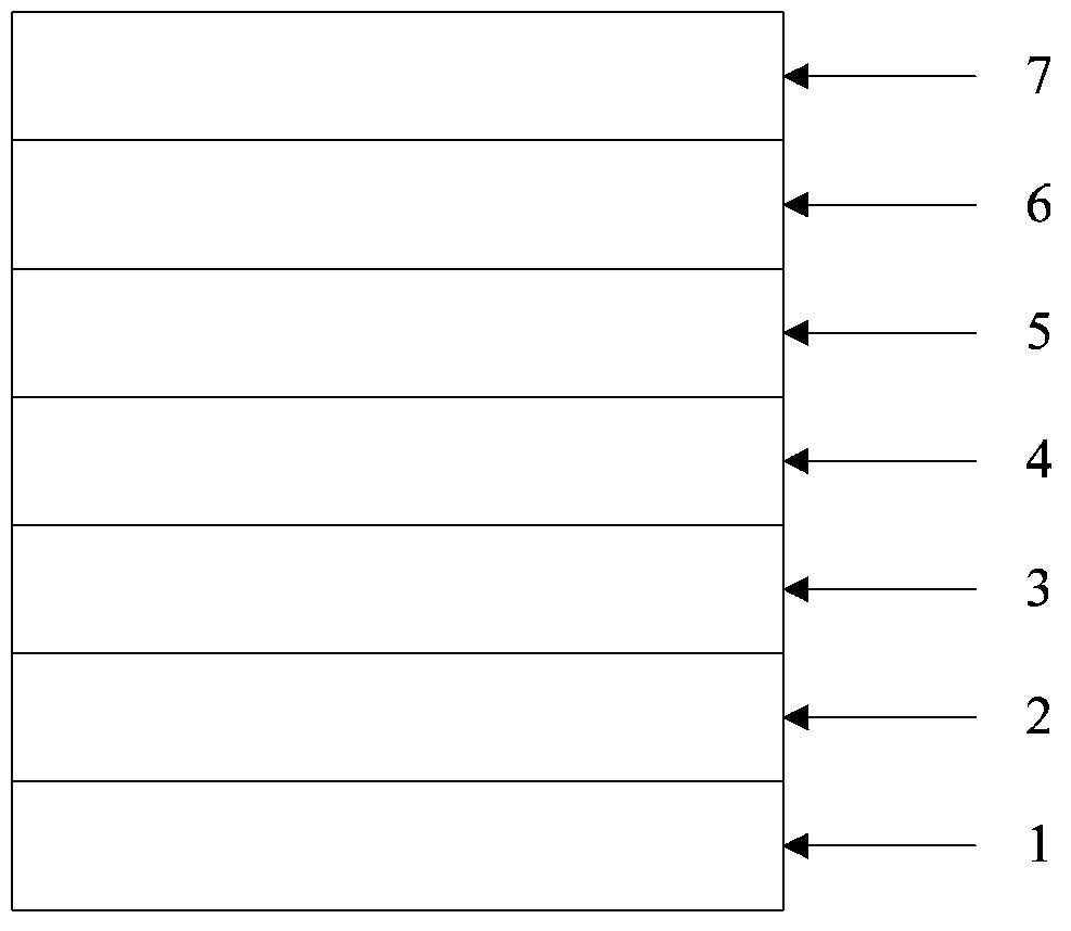
[0032] The preparation method of the above-mentioned inverted bottom emission organic electroluminescent device comprises the following steps:

[0033]S1. First, carry out photolithography treatment on the cathode substrate, cut it into the required size, and then clean the cathode substrate, that is, use detergent, deionized water, acetone, ethanol, and isopropanol to ultrasonically for 15 minutes each to remove the surface of the cathode substrate. Organic Pollutants;

[0034] S2. Coating an acetic acid compound solution with a mass concentration of 1 to 30% on the surface of the conductive cathode layer of the cathode base, and drying to obtain an auxiliary electron transport layer with a thickness of 10 to 20 nm; wherein, the material of the auxiliary electron transport layer is Acetic compounds such as zinc acetate (ZnAc), calcium acetate (CaAc) or magnesium acetate (MgAc);

[0035] S3, sequentially stacking and vapor-depositing an electron transport layer, a light-emitt...

Embodiment 1

[0042] First, the ITO glass is subjected to photolithography treatment, cut into the required size, and the organic pollutants on the surface of the ITO glass are removed with detergent, deionized water, acetone, ethanol, and isopropanol for 15 minutes each;

[0043] Then, spin-coat the auxiliary electron transport layer: first, ZnO is added to acetic acid, and Zn(Ac) with a mass concentration of 5% is configured. 2 solution; secondly, the Zn(Ac) 2 The solution was spin-coated on the surface of the ITO layer of ITO glass to control the thickness to 100nm, and then dried at 100°C to obtain Zn(Ac) 2 The auxiliary electron transport layer of the material;

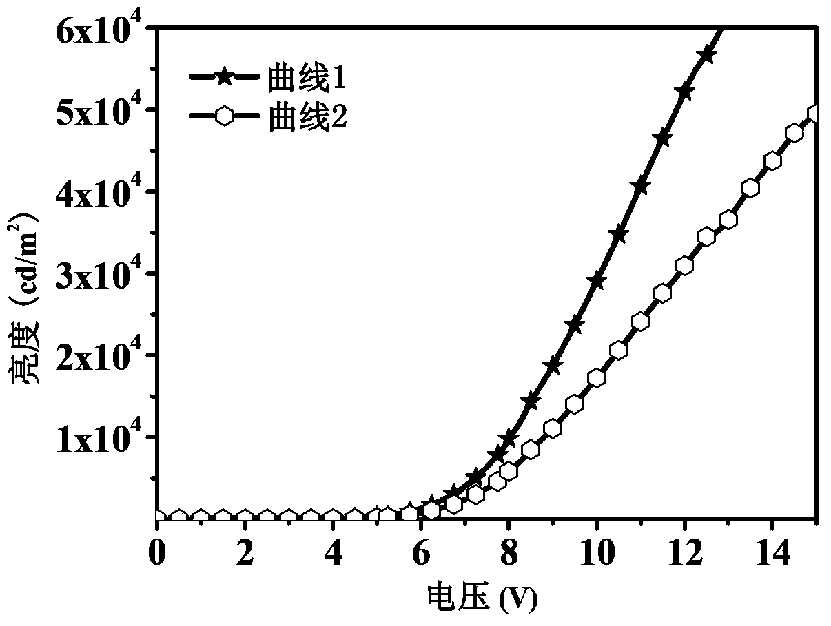
[0044] Next, on the surface of the auxiliary electron transport layer, the vapor-deposited electron transport layer, light-emitting layer, hole transport layer, hole injection layer and anode layer are stacked in sequence; the materials are: Bphen, TCTA:Ir(ppy) 3 (Represents Ir(ppy) 3 As a guest material doped into TCTA hos...

Embodiment 2

[0047] First, the IZO glass is photolithographically processed, cut into the required size, and then ultrasonicated for 15 minutes with detergent, deionized water, acetone, ethanol, and isopropanol to remove organic pollutants on the surface of the IZO glass;

[0048] Then, spin-coat the auxiliary electron transport layer: first add ZnO to acetic acid, and configure a Zn(Ac) with a mass concentration of 30%. 2 solution; secondly, the Zn(Ac) 2 The solution was spin-coated on the surface of the IZO layer of IZO glass to control the thickness to 200nm, and then dried at 100°C to obtain Zn(Ac) 2 The auxiliary electron transport layer of the material;

[0049] Next, on the surface of the auxiliary electron transport layer, the vapor-deposited electron transport layer (the material is TPBi with a thickness of 80nm), the light-emitting layer (the material is Ir(MDQ) 2 (acac) is doped into the NPB host material as a guest material, expressed as NPB:Ir(MDQ) 2 (acac), Ir(MDQ) 2 (aca...


PUM


Abstract

The invention belongs to the field of organic semiconductors and discloses an inverted bottom-emitting organic electroluminescence device and a manufacturing method thereof. The device comprises a cathode substrate, an auxiliary electronic transmission layer, an electronic transmission layer, a light-emitting layer, a hole transporting layer, a hole injection layer and an anode layer which are sequentially stacked. The auxiliary electronic transmission layer is made from an acetic acid compound, and the thickness of the auxiliary electronic transmission layer is 10-200nm. In the inverted bottom-emitting organic electroluminescence device, the electronic transmission speed of an inorganic material is several magnitude orders higher than that of an organic material, but the electronic transmission speed of an OLED is often 2-3 magnitude orders lower than that of holes. Therefore, the added auxiliary electronic transmission layer made from the acetic acid compound can well improve the electronic transmission speed, and the luminous efficiency of the device is improved greatly.

Description

technical field [0001] The invention relates to the field of organic semiconductors, in particular to an inverted bottom-emitting organic electroluminescence device and a preparation method thereof. Background technique [0002] In 1987, C.W.Tang and Van Slyke of Eastman Kodak Company in the United States reported a breakthrough in the research of organic electroluminescence. A high-brightness, high-efficiency double-layer organic electroluminescent device (OLED) has been prepared using ultra-thin film technology. In this double-layer structure device, the brightness reaches 1000cd / m at 10V 2 , its luminous efficiency is 1.51lm / W, and its lifespan is more than 100 hours. [0003] The principle of OLED light emission is based on the action of an external electric field, electrons are injected from the cathode to the lowest unoccupied molecular orbital (LUMO) of organic matter, and holes are injected from the anode to the highest occupied orbital (HOMO) of organic matter. E...

Claims


Application Information

Patent Timeline
Patent Type & Authority Applications(China)
IPC IPC(8): H01L51/50H01L51/56
CPCH10K50/166H10K50/854H10K2102/00H10K2102/321H10K71/00
Inventor 周明杰王平黄辉陈吉星
Owner OCEANS KING LIGHTING SCI&TECH CO LTD
Why Eureka
Try Eureka