Organic electroluminescence device and manufacturing method thereof

An electroluminescence device and a luminescence technology are applied in the direction of organic semiconductor devices, electric solid devices, chemical instruments and methods, etc., and can solve the problems of not making the thickness too thin, reducing the probability of exciton recombination, and exciton loss. Achieve the effect of increasing the electron transmission rate, enhancing the electron transmission, and increasing the probability of recombination

Inactive Publication Date: 2014-02-12
OCEANS KING LIGHTING SCI&TECH CO LTD +1
View PDF0 Cites 7 Cited by
  • Summary
  • Abstract
  • Description
  • Claims
  • Application Information

AI Technical Summary

Problems solved by technology

[0004] In traditional light-emitting devices, an electron transport layer is generally prepared to increase the electron transport rate, and an electron injection layer is prepared to improve the electron injection efficiency, and the electron transport rate is usually lower than the hole transport rate. Two or three orders of magnitude. Therefore, the electron transport layer is usually n-doped, that is, the electron transport layer is doped with metal, such as doping Cs salt into Bphen and Li salt into TPBi to improve Electron transfer rate, this method is widely used, and can effectively increase the electron transfer rate, but the rate increase is not high, and the thickness can not be made too thin (less than 40nm), when the luminescent material is relatively close to the metal electrode Sometimes, the luminescent material will be coupled with the metal electrode, which will cause loss of excitons (surface plasmon waves), the thickness is too thick (higher than 100nm), defects will increase, and the existence of electron traps will cause electrons or holes to enter the In the trap, the probability of exciton recombination is reduced; all of these affect the increase of electron transport rate, which leads to low luminous efficiency

Method used


Image

  • Organic electroluminescence device and manufacturing method thereof
  • Organic electroluminescence device and manufacturing method thereof

Examples


preparation example Construction

[0037] The preparation method of the above-mentioned organic electroluminescent device comprises the following steps:

[0038] S1. First carry out photolithographic treatment on the anode base, cut it into the required size, and then clean it. The cleaning process is to use detergent, deionized water, acetone, ethanol, and isopropanol to ultrasonically for 15 minutes each to remove the surface of the anode base. Organic Pollutants;

[0039] S2. Perform oxygen plasma treatment on the conductive anode layer of the cleaned anode base to increase the work function of the conductive anode layer of the anode base; the treatment time is 5-15min, and the treatment power is 10-50W;

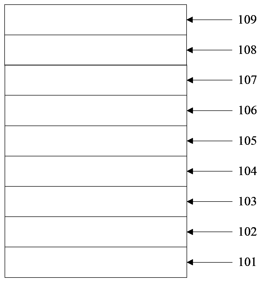
[0040] S3. In the vacuum coating equipment, sequentially vapor-deposit a hole injection layer, a hole transport layer, a light-emitting layer and a first electron transport layer on the conductive anode layer of the anode substrate;

[0041] S4. Then, electron beam evaporation is used to deposit a spacer ...

Embodiment 1

[0049] First, the ITO glass is washed with detergent, deionized water, and ultrasonic for 15 minutes to remove the organic pollutants on the surface of the ITO glass. After cleaning, the ITO layer of the ITO glass is treated with oxygen plasma. The treatment time is 5 minutes and the power is 50W;

[0050] Secondly, on the surface of the ITO layer after oxygen plasma treatment, the evaporated hole injection layer (the material is WO 3 , thickness is 40nm), hole transport layer (material is NPB, thickness is 40nm); light-emitting layer (material is Ir(ppy) 3 Doped into TCTA, expressed as TCTA:Ir(ppy) 3 , Ir(ppy) 3 The doping mass percentage is 10%; the thickness is 20nm), the first electron transport layer (the material is TAZ, the thickness is 60nm);

[0051] Then the electron beam evaporates the spacer layer: the material is ZnO, and the thickness is 40nm;

[0052] Then, on the surface of the spacer layer, the evaporation-assisted electron transport layer (made of ZnS with...

Embodiment 2

[0055] First, the ITO glass is washed with detergent, deionized water, and ultrasonic for 15 minutes to remove the organic pollutants on the surface of the ITO glass. After cleaning, the ITO layer of the ITO glass is treated with oxygen plasma. The treatment time is 15 minutes and the power is 10W;

[0056] Subsequently, on the surface of the ITO layer after oxygen plasma treatment, the evaporated hole injection layer (the material is MoO 3 , thickness is 20nm), hole transport layer (material is TAPC, thickness is 60nm), light-emitting layer (material is Ir(MDQ) 2 (acac) doped into NPB, expressed as NPB:Ir(MDQ) 2 (acac), Ir(MDQ) 2 (acac) doping mass percentage is 2%; thickness is 20nm), the first electron transport layer (material is TPBi, thickness is 40nm)

[0057] Then the electron beam evaporates the spacer layer, the material is MgO, and the thickness is 20nm;

[0058] Then, on the surface of the spacer layer, the vapor-deposited auxiliary electron transport layer (mat...


PUM

PropertyMeasurementUnit
Thicknessaaaaaaaaaa
Thicknessaaaaaaaaaa
Thicknessaaaaaaaaaa

Abstract

The invention belongs to the field of organic semiconductor materials and discloses an organic electroluminescence device and a manufacturing method of the organic electroluminescence device. The organic electroluminescence device comprises an anode substrate, a hole injection layer, a hole transmission layer, a light-emitting layer, a first electron transmission layer, a spacing layer, an auxiliary electron transmission layer, an electron injection layer and a cathode layer, wherein the anode substrate, the hole injection layer, the hole transmission layer, the light-emitting layer, the first electron transmission layer, the spacing layer, the auxiliary electron transmission layer, the electron injection layer and the cathode layer are sequentially stacked. The spacing layer is made of zinc oxide or titanium dioxide or magnesium oxide. According to the organic electroluminescence device, the auxiliary electron transmission layer is manufactured, so that transmission of electrons is enhanced; meanwhile, the spacing layer made of metallic oxide is arranged between the first electron transmission layer and the auxiliary electron transmission layer, photons are prevented from being coupled with the free electrons of metal electrodes to a certain degree, and therefore the light-emitting efficiency of the organic electroluminescence device is improved.

Description

technical field [0001] The invention relates to organic semiconductor materials, in particular to an organic electroluminescent device and a preparation method thereof. Background technique [0002] In 1987, C.W.Tang and Van Slyke of Eastman Kodak Company in the United States reported a breakthrough in the research of organic electroluminescence. A high-brightness, high-efficiency double-layer organic electroluminescent device (OLED) has been prepared using ultra-thin film technology. In this double-layer structure device, the brightness reaches 1000cd / m at 10V 2 , its luminous efficiency is 1.51lm / W, and its lifespan is more than 100 hours. [0003] The principle of OLED light emission is based on the action of an external electric field, electrons are injected from the cathode to the lowest unoccupied molecular orbital (LUMO) of organic matter, and holes are injected from the anode to the highest occupied orbital (HOMO) of organic matter. Electrons and holes meet, recom...

Claims


Application Information

Patent Timeline
IPC IPC(8): H01L51/52H01L51/54H01L51/56C09K11/06
CPCH10K50/166H10K50/18H10K50/854H10K2102/00H10K71/00
Inventor 周明杰王平黄辉陈吉星
Owner OCEANS KING LIGHTING SCI&TECH CO LTD
Why Eureka
Try Eureka