Top-emitting organic electroluminescent device and preparation method thereof

A technology of electroluminescence and top emission, which is applied in the fields of electric solid-state devices, semiconductor/solid-state device manufacturing, electrical components, etc. It can solve the problems of unfavorable carrier injection and insufficient transmittance, maintain stability and improve injection efficiency , the effect of high light extraction efficiency

Inactive Publication Date: 2014-02-19
OCEANS KING LIGHTING SCI&TECH CO LTD +2
View PDF0 Cites 6 Cited by
  • Summary
  • Abstract
  • Description
  • Claims
  • Application Information

AI Technical Summary

Problems solved by technology

At this time, a high-transmittance electrode is needed for top-emitting devices. Usually, thin-layer metal Ag and Al are used as transparent cathodes, but the transmittance of this thin film material is not high enough, and when ITO thin films are used as cathodes, due to work If the function is too high, it is not good for carrier injection

Method used


Image

  • Top-emitting organic electroluminescent device and preparation method thereof
  • Top-emitting organic electroluminescent device and preparation method thereof

Examples


Embodiment 1

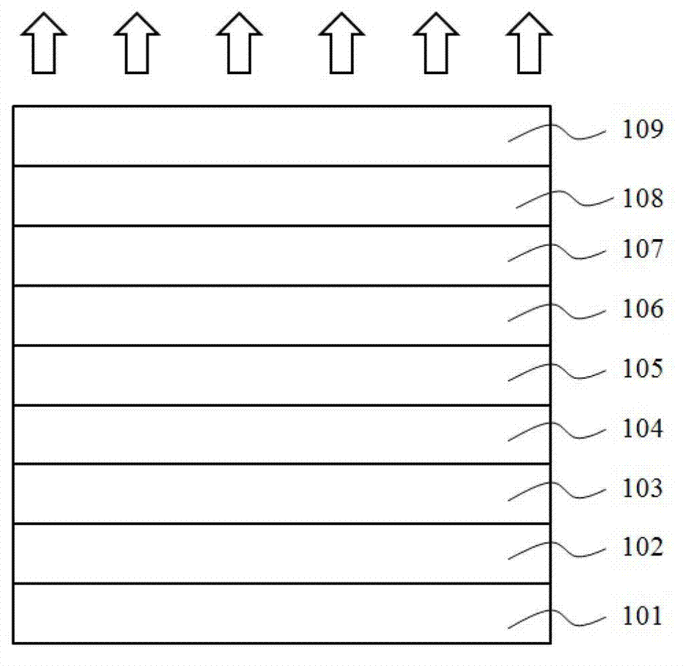
[0050] The structure of the top emission organic electroluminescent device of this embodiment is: glass / Al / LiN 3 :Alq 3 / BAlq / NPB:Ir(MDQ) 2 (acac) / NPB / F4-TCNQ:m-MTDATA / ReO 3 / ITO

[0051] The fabrication method of the top emission organic electroluminescent device is as follows:

[0052] 1. Use detergent, deionized water, isopropanol, and acetone to ultrasonically clean the glass substrate for 20 minutes, and then dry it with nitrogen;

[0053] 2. After the glass is cleaned, it is placed in a vacuum thermal sputtering system, and the cathode layer (the material is Al, the thickness is 70nm), the electron transport layer (the material is LiN 3 Doped to Alq at a mass ratio of 5% 3 , expressed as LiN 3 :Alq 3 ; thickness is 30nm), hole blocking layer (material is BAlq; thickness is 10nm), light-emitting layer (material is Ir(MDQ) 2 (acac) is doped into the NPB host material as a dopant material, expressed as NPB:Ir(MDQ) 2 (acac), Ir(MDQ) 2 (acac) doping mass ratio is 5%...

Embodiment 2

[0056] The top-emitting organic electroluminescent device of this embodiment has a structure of: glass / Ag / CsN 3 :Bphen / BPhen / CBP:FIrPic / TPD / F4-TCNQ:MeO-TPD / WO 3 / IZO

[0057] The fabrication method of the top emission organic electroluminescent device is as follows:

[0058] 1. Use detergent, deionized water, isopropanol, and acetone to ultrasonically clean the glass substrate for 20 minutes, and then dry it with nitrogen;

[0059] 2. After the glass is cleaned, it is placed in a vacuum thermal sputtering system, and the cathode layer (the material is Ag with a thickness of 100nm) and the electron transport layer (the material is CsN) are sequentially evaporated on the glass surface. 3 Doped into Bphen at a mass ratio of 30%, expressed as CsN 3 : Bphen; the thickness is 60nm), the hole blocking layer (the material is BPhen; the thickness is 10nm), the light-emitting layer (the material is FIrPic is doped into the CBP host material as the doping material, expressed as CBP: F...

Embodiment 3

[0062] The top emission organic electroluminescent device of the present embodiment has a structure of: glass / Ag-Mg / Li 2 CO 3 :TPBi / TPBi / NPB:Ir(MDQ) 2 (acac) / TPD / F4-TCNQ:2-TNATA / MoO 3 / AZO

[0063] The fabrication method of the top emission organic electroluminescent device is as follows:

[0064] 1. Use detergent, deionized water, isopropanol, and acetone to ultrasonically clean the glass substrate for 20 minutes, and then dry it with nitrogen;

[0065] 2. After the glass is cleaned, it is placed in a vacuum thermal sputtering system, and the cathode layer (the material is Ag-Mg, the thickness is 200nm), the electron transport layer (the material is Li 2 CO 3 Doped into TPBi according to the mass ratio of 20%, expressed as Li 2 CO 3 :TPBi; thickness is 10nm), hole blocking layer (material is TPBi; thickness is 40nm), light emitting layer (material is Ir(MDQ) 2 (acac) is doped into the NPB host material as a dopant material, expressed as NPB:Ir(MDQ) 2 (acac), Ir(MDQ) ...


PUM

PropertyMeasurementUnit
thicknessaaaaaaaaaa
thicknessaaaaaaaaaa
thicknessaaaaaaaaaa

Abstract

The invention belongs to the field of organic semiconductor materials and discloses a top-emitting organic electroluminescent device and a preparation method thereof. The device comprises a substrate, a cathode layer, an electronic transmission layer, a hole barrier layer, a luminescent layer, an electronic barrier layer, a hole transmission layer, a buffer layer and an anode layer which are successively stacked. The buffer layer is made of rhenium trioxide, rhenium heptoxide, tungsten oxide, molybdenum trioxide, molybdenum dioxide or vanadic oxide. According to the top-emitting organic electroluminescent device, metal is employed as a cathode and a transparent conductive oxide is employed as an anode so that the carrier injection problem is solved, and the anode can be placed at the top of the luminescent device as a light extraction direction so as to obtain quite high light extraction efficiency; besides, the buffer layer is arranged between the anode and an organic layer and is provided with quite high work content sot that the hole injection efficiency can be improved.

Description

technical field [0001] The invention relates to the field of organic semiconductor materials, in particular to a top-emitting organic electroluminescence device and a preparation method thereof. Background technique [0002] Organic Light Emission Diode, hereinafter referred to as OLED, has the characteristics of high brightness, wide range of material selection, low driving voltage, fully cured active light emission, etc., and has the advantages of high definition, wide viewing angle, and fast response speed. It is a display technology and light source with great potential, which conforms to the development trend of mobile communication and information display in the information age, as well as the requirements of green lighting technology, and is the focus of many researchers at home and abroad. [0003] Organic electroluminescent diodes have a sandwich-like structure, with a cathode and an anode at the top and bottom, and a single or multiple functional layers of organic ...

Claims


Application Information

Patent Timeline
Patent Type & Authority Applications(China)
IPC IPC(8): H01L51/52H01L51/50H01L51/56
CPCH10K50/17H10K50/81H10K50/82H10K71/00
Inventor 周明杰王平冯小明张振华
Owner OCEANS KING LIGHTING SCI&TECH CO LTD
Why Eureka
Try Eureka