Organic electroluminescent device and preparation method thereof

An electroluminescent device and luminescent technology, which is applied in the direction of electric solid-state devices, semiconductor/solid-state device manufacturing, electrical components, etc., can solve the problems of low device life, low luminous efficiency, and large current to drive light-emitting devices, and achieve device life. Improve, improve luminous efficiency, reduce the effect of injection barrier

Inactive Publication Date: 2014-02-19
OCEANS KING LIGHTING SCI&TECH CO LTD +2
View PDF0 Cites 33 Cited by
  • Summary
  • Abstract
  • Description
  • Claims
  • Application Information

AI Technical Summary

Problems solved by technology

[0004] So far, although researchers from all over the world have greatly improved the performance indicators of the device by selecting suitable organic

Method used


Image

  • Organic electroluminescent device and preparation method thereof
  • Organic electroluminescent device and preparation method thereof

Examples


Embodiment 1

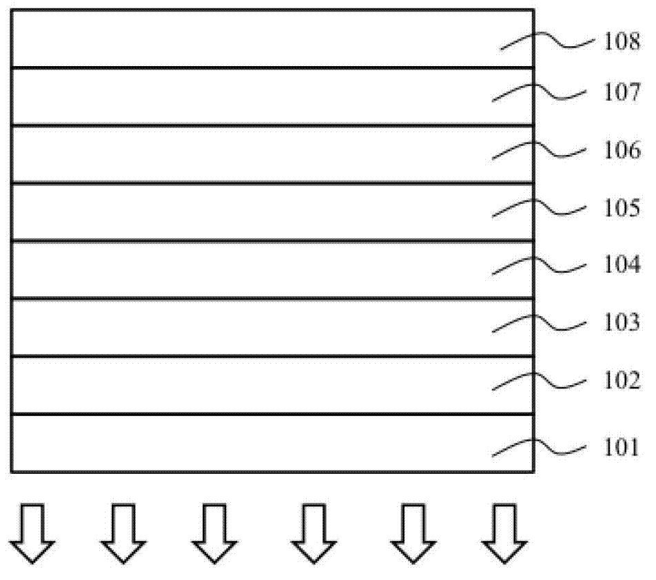
[0045] The organic electroluminescent device of the present embodiment has a structure of: glass / ITO / CuPc / NPB / NPB:Ir(MDQ) 2 (acac) / TPBi / Sm:TPBi / Ag

[0046] The fabrication method of the organic electroluminescent device is as follows:

[0047] 1. Use detergent, deionized water, isopropanol, and acetone to ultrasonically clean the glass substrate for 20 minutes, and then dry it with nitrogen;

[0048] 2. After cleaning the glass substrate, put it into a vacuum magnetron sputtering system to prepare an anode layer with a thickness of 100nm and made of ITO on the glass surface. At this time, ITO and glass are combined together, referred to as ITO glass; then , place the ITO glass in the plasma treatment chamber, and perform plasma treatment on the ITO layer to improve the work function of the anode layer and reduce the hole injection barrier;

[0049] 3. Place the ITO glass after oxygen plasma treatment in the vacuum thermal coating system, and stack the evaporated hole injecti...

Embodiment 2

[0053] The organic electroluminescent device of the present embodiment has a structure of: glass / ITO / ZnPc / TCTA / TCTA:Ir(ppy) 3 / BAlq / Sr:Alq 3 / Al

[0054] The fabrication method of the organic electroluminescent device is as follows:

[0055] 1. Use detergent, deionized water, isopropanol, and acetone to ultrasonically clean the glass substrate for 20 minutes, and then dry it with nitrogen;

[0056] 2. After cleaning the glass substrate, put it into a vacuum magnetron sputtering system to prepare an anode layer with a thickness of 100nm and made of ITO on the glass surface. At this time, ITO and glass are combined together, referred to as ITO glass; then , place the ITO glass in the plasma treatment chamber, and perform plasma treatment on the ITO layer to improve the work function of the anode layer and reduce the hole injection barrier;

[0057] 3. Place the ITO glass after oxygen plasma treatment in the vacuum thermal coating system, and stack the evaporated hole injectio...

Embodiment 3

[0061] The organic electroluminescent device of this embodiment has a structure of: glass / ITO / m-MTDATA / TPD / TCTA:Ir(ppy) 3 / BAlq / Yb:BAlq / Al-Mg

[0062] The fabrication method of the organic electroluminescent device is as follows:

[0063] 1. Use detergent, deionized water, isopropanol, and acetone to ultrasonically clean the glass substrate for 20 minutes, and then dry it with nitrogen;

[0064] 2. After cleaning the glass substrate, put it into a vacuum magnetron sputtering system to prepare an anode layer with a thickness of 100nm and made of ITO on the glass surface. At this time, ITO and glass are combined together, referred to as ITO glass; then , place the ITO glass in the plasma treatment chamber, and perform plasma treatment on the ITO layer to improve the work function of the anode layer and reduce the hole injection barrier;

[0065] 3. Place the ITO glass after oxygen plasma treatment in the vacuum thermal coating system, and stack the evaporated hole injection la...


PUM

PropertyMeasurementUnit
Thicknessaaaaaaaaaa
Thicknessaaaaaaaaaa
Thicknessaaaaaaaaaa

Abstract

The invention belongs to the field of organic semiconductor materials and discloses an organic electroluminescent device and a preparation method thereof. The device comprises an anode layer, a hole injection layer, a hole transmission layer, a luminescent layer, a hole barrier layer, an electronic barrier layer and a cathode layer which are successively stacked. The electronic transmission layer is made of a doped mixing material which is prepared by doping a metal doping agent to an electronic transmission matrix material according to a mass ratio of 10 to 50%. According to the organic electroluminescent device, the metal doping agent in the electronic transmission layer can effectively enable the electrons of a metal material to be transferred to the LUMO energy level of the electronic transmission matrix material so as to enhance the conductivity of the electronic transmission matrix material. Besides, ohmic contact is enabled to be formed between the electronic transmission matrix material and a cathode, the injection barrier of the electrons is reduced, the starting voltage of the device is reduced at the same time, the luminescence efficiency of the device is improved, the driving current of the device is small, and the service life of the device is prolonged.

Description

technical field [0001] The invention relates to the field of organic semiconductor materials, in particular to an organic electroluminescence device and a preparation method thereof. Background technique [0002] Organic Light Emission Diode, hereinafter referred to as OLED, has the characteristics of high brightness, wide range of material selection, low driving voltage, fully cured active light emission, etc., and has the advantages of high definition, wide viewing angle, and fast response speed. It is a display technology and light source with great potential, which conforms to the development trend of mobile communication and information display in the information age, as well as the requirements of green lighting technology, and is the focus of many researchers at home and abroad. [0003] Organic electroluminescent diodes have a sandwich-like structure, with a cathode and an anode at the top and bottom, and a single or multiple functional layers of organic materials of...

Claims


Application Information

Patent Timeline
IPC IPC(8): H01L51/54H01L51/50H01L51/56
CPCH10K50/165H10K71/00
Inventor 周明杰王平冯小明张振华
Owner OCEANS KING LIGHTING SCI&TECH CO LTD
Why Eureka
Try Eureka