Method for preparing GaN basal keel type laser diode

A laser diode and ridge-type technology, which is applied in the direction of lasers, laser components, semiconductor lasers, etc., can solve the problems of difficult control of the opening conditions of the insulating layer, and difficulty in aligning the electrode windows of the ridge-type laser diode, so as to avoid the process of plate alignment , save equipment and manpower input, and achieve regular effects

Active Publication Date: 2014-03-05
北京燕园中镓半导体工程研发中心有限公司 +1
View PDF5 Cites 2 Cited by
  • Summary
  • Abstract
  • Description
  • Claims
  • Application Information

AI Technical Summary

Problems solved by technology

[0004] The purpose of the present invention is to provide a preparation method of a ridge-type GaN-based laser diode, which can simultaneously solve the two major problems of the current ridge-type laser diode electrode window alignment difficulty and the opening conditions of the insulating layer are difficult to control

Method used


Image

  • Method for preparing GaN basal keel type laser diode
  • Method for preparing GaN basal keel type laser diode
  • Method for preparing GaN basal keel type laser diode

Examples


Embodiment 1

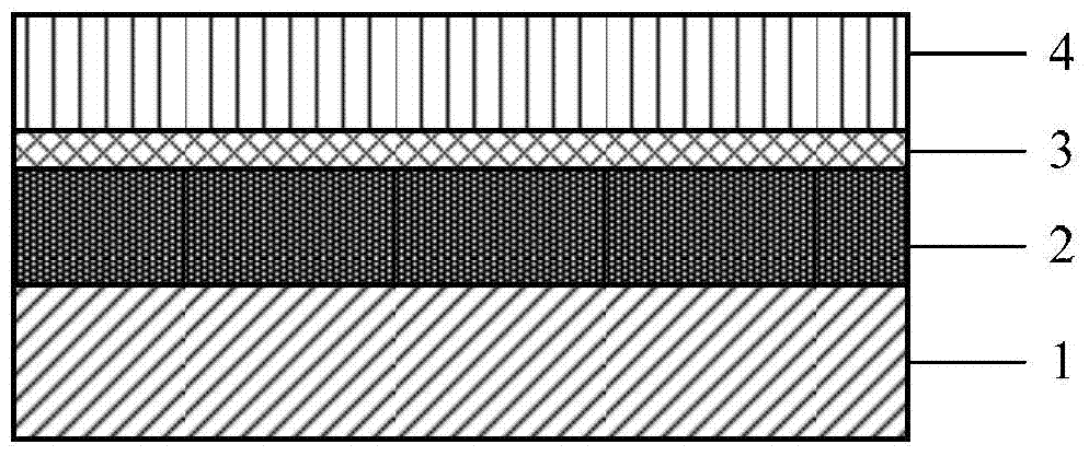
[0029] A GaN-based LD epitaxial layer 2 grown on a back-polished sapphire substrate 1, on the front of the GaN-based LD epitaxial layer 2, Ni / Au is deposited as a light-shielding layer 3 by electron beam deposition, and a photoresist is coated with a coater 4, such as Picture 1-1 shown.

[0030] Use a ridge photolithography plate to expose, develop, and remove the base film with a plasma stripper to form a strip photoresist 4, such as Figure 1-2 shown.

[0031] Use Ni / Au etching solution to etch the Ni / Au not protected by photoresist at room temperature, and the remaining Ni / Au light-shielding layer is strip-shaped 3, such as Figure 1-3 shown.

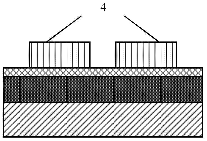
[0032] Use ICP to etch out the P-region ridge structure 5 of the laser diode, such as Figure 1-4 shown.

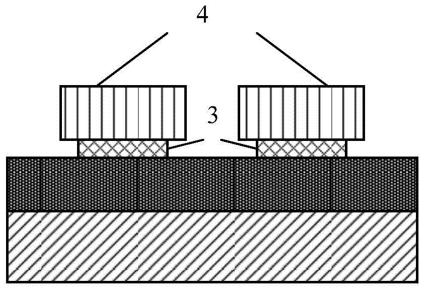
[0033] Clean the photoresist 4, and then anneal the alloy to form an ohmic contact, such as Figure 1-5 shown.

[0034] Coat the photoresist 6 with a glue leveler, use an N-type mesa photolithography plate to pass throug...

Embodiment 2

[0046] A GaN-based LD epitaxial layer 2 grown on a back-polished gallium nitride substrate, on the front side of the GaN-based LD epitaxial layer 2, Ni / Au is deposited as a light-shielding layer 3 by electron beam, and the photolithographic layer is coated with a coater Glue 4, such as diagram 2-1 shown.

[0047] Use a ridge photolithography plate to expose, develop, and remove the bottom film with a plasma stripper to form a strip photoresist, such as Figure 2-2 shown.

[0048] Use Ni / Au etching solution to etch the Ni / Au not protected by photoresist at room temperature, and the remaining Ni / Au light-shielding layer is strip-shaped 3, such as Figure 2-3 shown.

[0049] Use ICP to etch out the P-region ridge structure 5 of the laser diode, such as Figure 2-4 shown.

[0050] Clean the photoresist 4, and then anneal the alloy to form an ohmic contact, such as Figure 2-5 shown.

[0051] Apply a negative photosensitive heat-curing polyimide coating glue 10 on the epita...


PUM


Abstract

The invention discloses a method for preparing a GaN basal keel type laser diode. The method comprises the following steps: firstly, using a P-area contact metal electrode as a light blocking layer on the top of a keel before the keel is subjected to dry etching, subsequently coating a negative photosensitivity thermocuring coating adhesive by using a spinning coating technique; secondly, performing secondary photoetching by using a back exposure technique, wherein the light blocking layer can effectively prevent the photoresist on the top of the keel from being exposed by ultraviolet light, so that photoetched patterns are achieved; finally, obtaining an insulating layer with complete and regular structure through a high-temperature curing method according to the properties of the negative photosensitivity thermocuring coating adhesive. The method has the characteristics that the problems that the conventional keel laser electrode windows are difficult to align and the insulating layer windowing condition is difficult to control are solved.

Description

technical field [0001] The invention belongs to the field of optoelectronic technology, and in particular relates to a preparation method of a GaN-based laser diode (LD). Background technique [0002] GaN (gallium nitride) based laser diode (LD) devices as optoelectronic devices have a wide range of applications and a huge product market. Optical storage and optical communication are currently the most important applications of semiconductor laser diodes. For optical discs, because the possible capacity of recording and reproduction is inversely proportional to the second power of the wavelength of the light source, it is necessary to shorten the wavelength of the laser light source to achieve high-density optical storage. The blue-violet GaN-based LD with a wavelength of 405 nanometers (nm) is the core device of a new generation of DVD in the field of high-density optical information storage, that is, the Blu-ray Disc; GaN-based blue and green light-emitting diodes have ma...

Claims


Application Information

Patent Timeline
Patent Type & Authority Applications(China)
IPC IPC(8): H01S5/343H01S5/22
Inventor 孟令海康香宁刘宁炀陈景春吴勇刘诗宇胡晓东
Owner 北京燕园中镓半导体工程研发中心有限公司
Why Eureka
Try Eureka