Formation method for transistor

A transistor and gas technology, used in semiconductor devices, semiconductor/solid-state device manufacturing, electrical components, etc., can solve problems such as unstable performance of transistors, and achieve the effect of stable performance

Active Publication Date: 2014-03-12
SEMICON MFG INT (SHANGHAI) CORP
View PDF6 Cites 13 Cited by
  • Summary
  • Abstract
  • Description
  • Claims
  • Application Information

AI Technical Summary

Problems solved by technology

[0005] However, the transistor performance of the high-K / metal gate structure formed by the prior art is not stable

Method used


Image

  • Formation method for transistor
  • Formation method for transistor
  • Formation method for transistor

Examples


no. 1 example

[0047] Figure 7 to Figure 10 It is a schematic cross-sectional structure diagram of the first embodiment of the formation process of the transistor of the present invention.

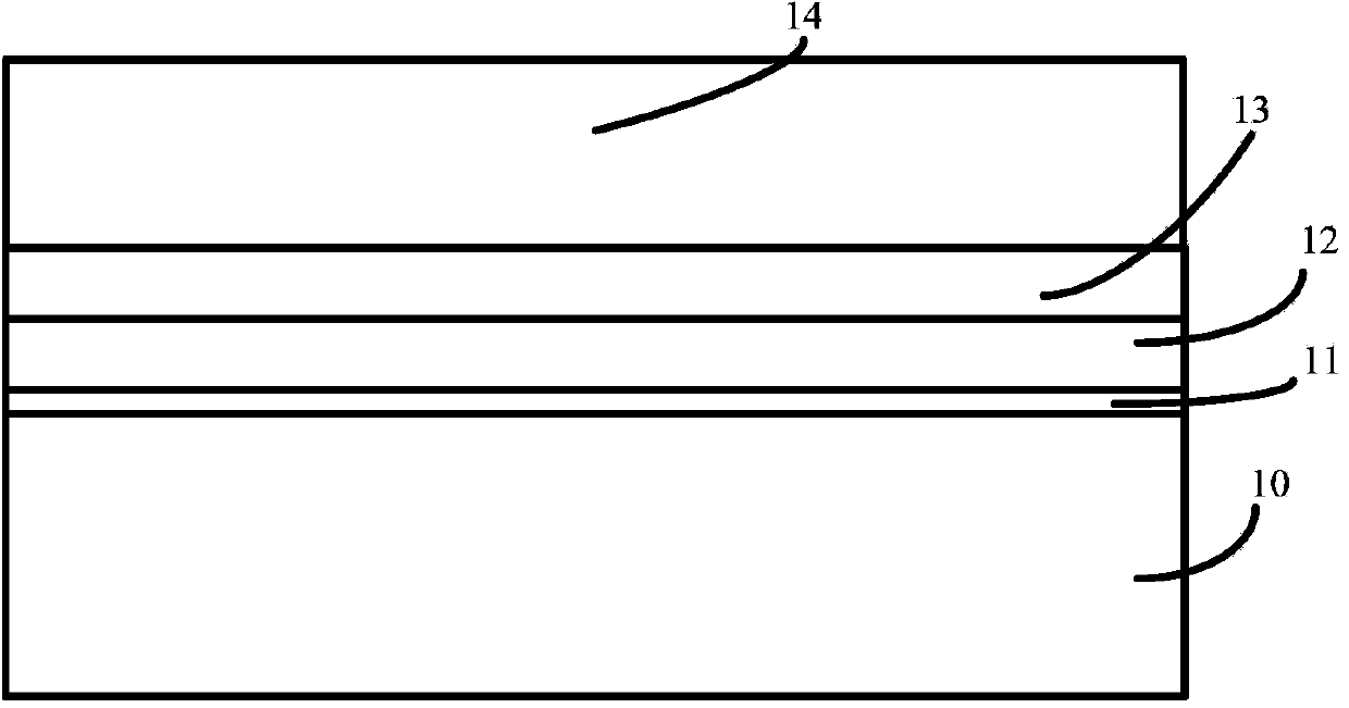
[0048] Please refer to Figure 7 , providing a semiconductor substrate 200; forming an insulating film 201 on the surface of the semiconductor substrate 200, a high-K dielectric film 202 on the surface of the insulating film 201, a protective film 203 on the surface of the high-K dielectric film 202, and a The gate electrode film 204 on the surface of the protection film 203 .

[0049] The semiconductor substrate 200 is used to provide a working platform for subsequent processes, and the material of the semiconductor substrate 200 is silicon, silicon germanium, silicon carbide, silicon-on-insulator or III-V compounds (silicon nitride or gallium arsenide, etc. ).

[0050] The material of the insulating film 201 is silicon oxide, and the forming process is a thermal oxidation process or a chemical vapo...

no. 2 example

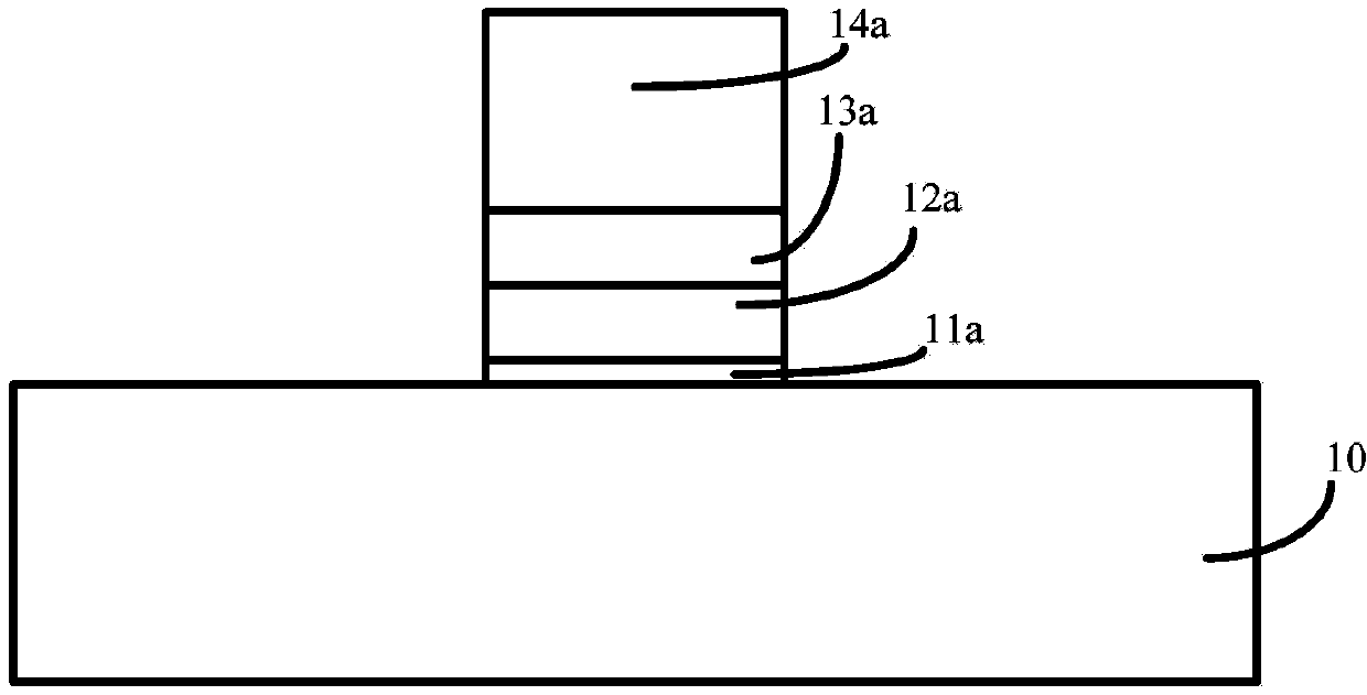
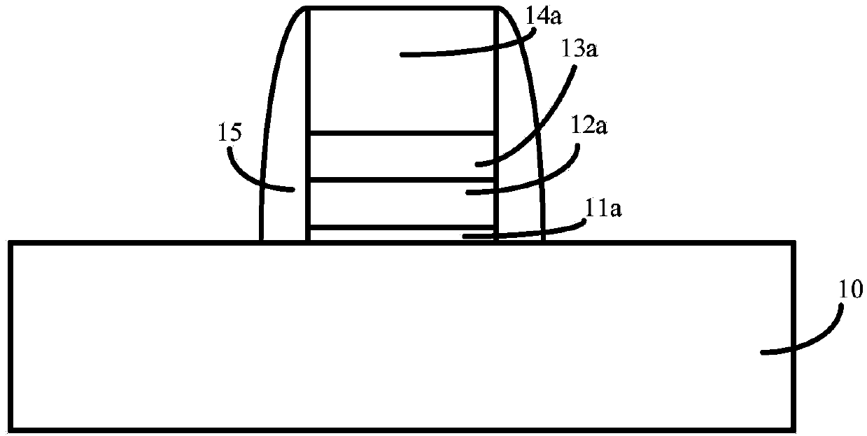
[0075] Figure 11 to Figure 13 It is a schematic cross-sectional structure diagram of the second embodiment of the formation process of the transistor of the present invention.

[0076] Please refer to Figure 11 , providing a semiconductor substrate 300; on the surface of the semiconductor substrate 300, an insulating layer 301, a high-K dielectric layer 302 located on the surface of the insulating layer 301, and a The protective layer 303, and the gate electrode layer 304 located on the surface of the protective layer 303; after etching, the gate electrode layer 304, the protective layer 303, the high-K dielectric layer 302 and the insulating layer 301 are cleaned; after cleaning , performing thermal annealing, the gas of the thermal annealing is hydrogen; and, after cleaning, forming First spacers 305; after thermal annealing and formation of first spacers 305, lightly doped regions 306 are formed on both sides of the gate electrode layer 304 and first spacers 305; after ...


PUM


Abstract

Provided is a formation method for a transistor. The formation method comprises that: a semiconductor substrate is provided; a high-K dielectric film is formed on the surface of the semiconductor substrate, and a gate electrode film is formed on the surface of the high-K dielectric film; part of the gate electrode film and the high-K dielectric film are etched so that a gate electrode layer and a high-K dielectric layer are formed; the gate electrode layer and the high-K dielectric layer are cleaned; after cleaning, thermal annealing is performed, wherein gas used for annealing is hydrogen; after cleaning, first side walls are formed on the surfaces of the semiconductor substrate of two sides of the gate electrode layer and the high-K dielectric layer; and after terminal annealing and after the first side walls are formed, source regions or drain regions are formed on the two sides of the first side wall of the gate electrode layer. The formed transistor is stable is performance.

Description

technical field [0001] The invention relates to the technical field of semiconductor manufacturing, in particular to a method for forming a transistor. Background technique [0002] With the rapid development of integrated circuit manufacturing technology, the size of semiconductor devices in integrated circuits, especially MOS (Metal Oxide Semiconductor, metal-oxide-semiconductor) devices, has been continuously reduced to meet the miniaturization and development of integrated circuits. Integration requirements. In the process of continuous shrinking of the size of MOS transistor devices, the process of using silicon oxide or silicon oxynitride as the gate dielectric layer in the existing process is challenged. Transistors formed with silicon oxide or silicon oxynitride as the gate dielectric layer have some problems, including increased leakage current and diffusion of impurities, which affect the threshold voltage of the transistor and further affect the performance of se...

Claims


Application Information

Patent Timeline
Patent Type & Authority Applications(China)
IPC IPC(8): H01L21/336
CPCH01L21/28158H01L21/28247H01L29/66477
Inventor 何有丰
Owner SEMICON MFG INT (SHANGHAI) CORP
Why Eureka
Try Eureka