Method for preparing h-BN medium graphene integrated circuits on large scale

A large-scale graphene technology, applied in the manufacture of circuits, electrical components, semiconductors/solid-state devices, etc., can solve problems such as low yield, high process difficulty, and poor performance, so as to improve performance, simplify the process, and promote development Effect

Inactive Publication Date: 2014-03-12
XIDIAN UNIV
View PDF4 Cites 22 Cited by
  • Summary
  • Abstract
  • Description
  • Claims
  • Application Information

AI Technical Summary

Problems solved by technology

This technology can overcome the problems of high process difficulty, low yield and poor performance in the current large-sc

Method used


Image

  • Method for preparing h-BN medium graphene integrated circuits on large scale
  • Method for preparing h-BN medium graphene integrated circuits on large scale
  • Method for preparing h-BN medium graphene integrated circuits on large scale

Examples


Embodiment

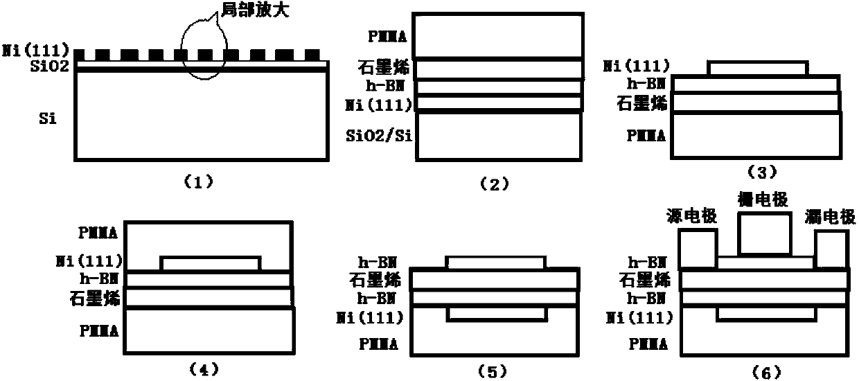
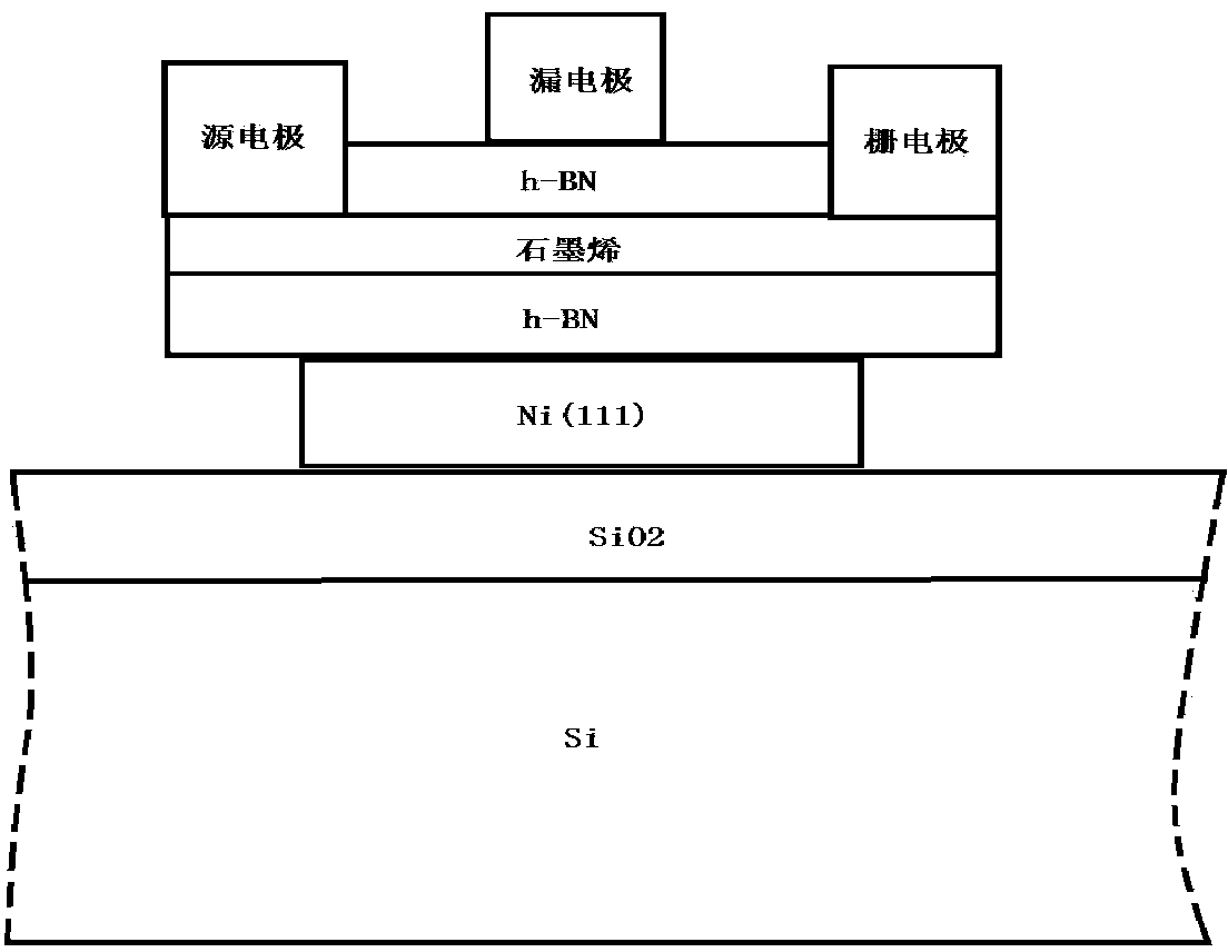
[0040] Embodiment: the preparation of large-scale h-BN dielectric graphene integrated circuit

[0041] In making large-scale h-BN dielectric graphene integrated circuits, the present invention takes the following technical solutions:

[0042] 1. Making SiO2 2 / Si substrate: 300nm SiO grown on a 4-inch Si wafer by dry oxidation 2 film;

[0043] 2. Catalytic metal layer growth: using electron beam evaporation process on SiO 2 A layer of Ni(111) film with a thickness of 250nm was grown on the Si substrate;

[0044] 3. Catalytic metal layer photolithography: use standard photolithography process to photolithographically prepare the catalytic metal layer on the Si wafer, each with a square catalytic metal pattern;

[0045]4. Bottom layer h-BN medium growth: use CVD method to selectively grow a layer of hexagonal boron nitride (h-BN) on the Ni(111) layer, with a thickness of about 20nm, and the grown h-BN pattern is similar to Ni(111) ) with the same graphics;

[0046] 5. Grap...


PUM

PropertyMeasurementUnit
Thicknessaaaaaaaaaa
Thicknessaaaaaaaaaa
Thicknessaaaaaaaaaa

Abstract

The invention belongs to the field of semiconductor devices and semiconductor processes, and aims to provide a method for preparing h-BN medium graphene integrated circuits on a large scale. In the method, a catalytic metal layer is subjected to photoetching by using the characteristic of selective growth of h-BN and graphene on a catalytic metal substrate, and control on the patterns of an h-BN layer and a graphene layer growing in an epitaxial way is realized, so that large-scale manufacturing of graphene field effect transistors taking the h-BN as a medium is realized. According to the method, the problems of high process difficulty, low yield and poor performance in the large-scale preparation process of graphene devices are solved, and a good basis is laid for the preparation of the graphene-based integrated circuits.

Description

Technical field: [0001] The invention relates to a h-BN dielectric graphene integrated circuit manufacturing technology, in particular to a large-scale manufacturing technology of a double-gate graphene field effect transistor using h-BN as a dielectric. Background technique: [0002] Graphene is a two-dimensional material with extremely excellent performance formed by carbon atoms in a hexagonal honeycomb lattice. Its carrier velocity and mobility are much higher than conventional semiconductor materials. It is considered as an integrated circuit material in the post-silicon era. Currently, large-scale graphene wafers can be grown by CVD on catalytic metal substrates and SiC epitaxy. In the preparation of graphene electronic devices, either the graphene prepared by CVD method needs to be transferred to SiO 2 / Si (or other) substrates, or directly use the 6H-SiC substrate as the dielectric layer. These substrates not only have a certain surface roughness, but also have a la...

Claims


Application Information

Patent Timeline
IPC IPC(8): H01L21/82H01L21/336B82Y10/00
CPCH01L21/8256H01L29/66015
Inventor 张鹏马中发吴勇庄奕琪赵钰迪冯元博陈祎坤
Owner XIDIAN UNIV
Why Eureka
Try Eureka