Wire electrode array structure preparation method for micro-electrochemical machining

An array structure, micro-electrolysis technology, applied in the direction of processing electrodes, electric processing equipment, electrode manufacturing, etc., can solve the problems of low processing efficiency, difficulty in processing high aspect ratio microstructures, and insufficient processing accuracy, and achieve the improvement of steepness, Improve localization and improve the effect of steepness

Active Publication Date: 2014-04-09
江苏蔚之领域智能科技有限公司
View PDF5 Cites 22 Cited by
  • Summary
  • Abstract
  • Description
  • Claims
  • Application Information

AI Technical Summary

Problems solved by technology

[0009] The purpose of the present invention is to provide a method for preparing a wire electrode array structure for micro electrolytic machining, which solves the problems of low processing efficiency, insufficient processing precision and difficulty in processing high aspect ratio microstructures in the micro electrolytic machining process of the prior art. question

Method used


Image

  • Wire electrode array structure preparation method for micro-electrochemical machining
  • Wire electrode array structure preparation method for micro-electrochemical machining
  • Wire electrode array structure preparation method for micro-electrochemical machining

Examples


preparation example Construction

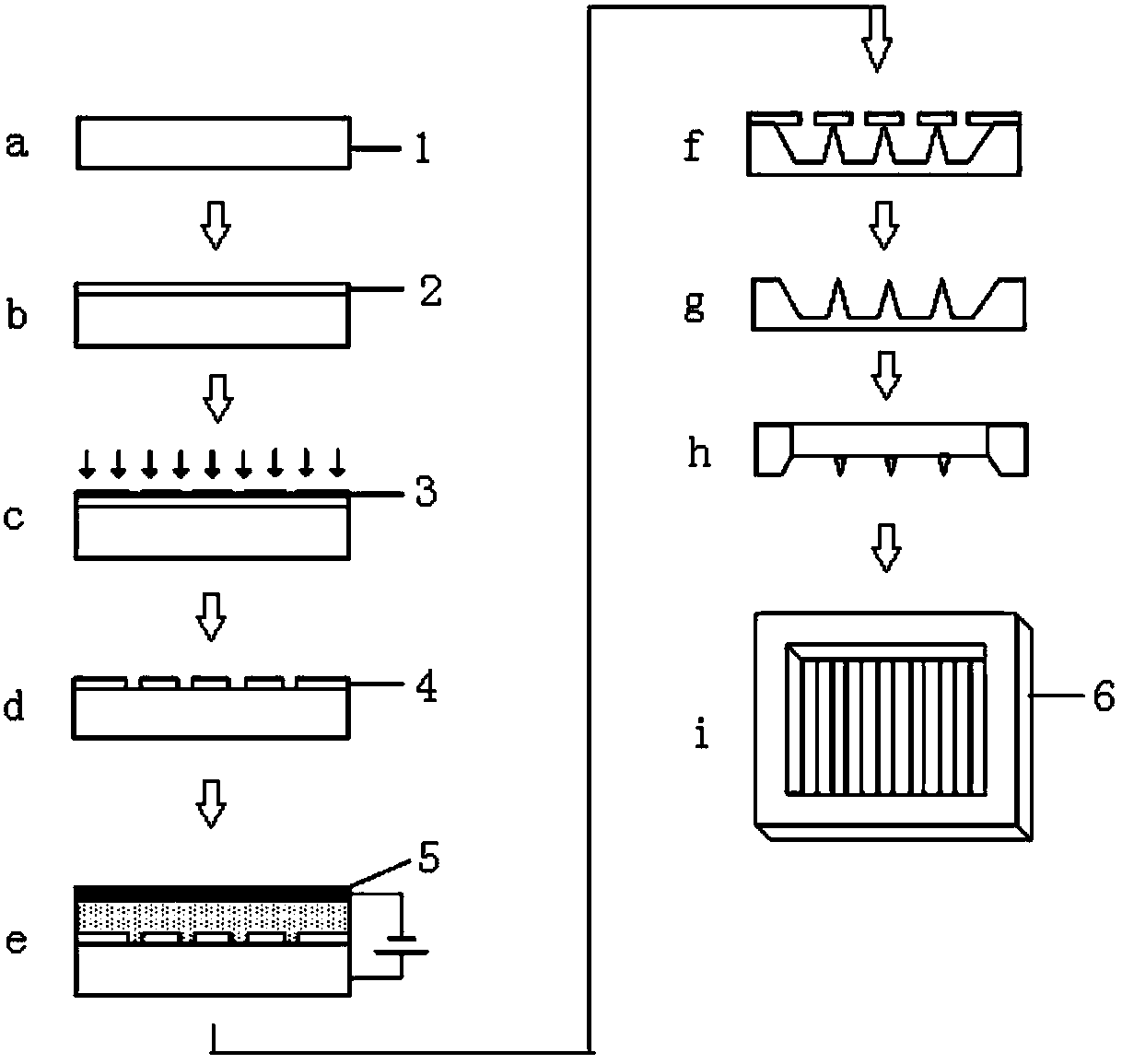
[0035] refer to figure 1 , the method for preparing a wire electrode array structure for micro-electrolytic machining of the present invention (describing the process of mask electrolytic deep etching combined with removal of back material to prepare wire electrodes), specifically includes the following steps:

[0036] Step 1. Pretreatment of the metal substrate: the metal substrate 1 is made of copper material. The purpose of the treatment is to make the surface of the sample smooth, clean and dry, and to be able to better adhere to the photoresist. The specific method is to polish the metal substrate 1 on a polishing machine. Polishing treatment to make the surface roughness Ra≤0.3, then use acetone, alcohol and deionized water to clean in sequence, then blow dry with nitrogen and dry on the dryer for use (see figure 1 a).

[0037] Step 2. Fabrication of patterned masking film for mask electrolytic processing: the masking film needs to have good electrical insulation. In th...

Embodiment

[0049] refer to Figure 4 , is the application of the electrode made by the method of the present invention, adopts the wire electrode array of the present invention to carry out metal microstructure array processing, implements according to the following steps:

[0050] Step 1, workpiece preparation ( Figure 4 a): The surface of the workpiece 10 to be processed is polished, cleaned, and dried for use;

[0051] Step 2, tool electrode preparation ( Figure 4 b): Using the above-mentioned wire electrode array manufacturing method (for the process principle, see figure 1 ) to make a wire electrode with integrated wire and frame, and control the distance between the wire electrode wires by controlling the width of the photoresist masking film during wire electrode fabrication, so that when the above wire electrode is used for electrolytic machining, the wire electrode The influence of mutual stray corrosion between them is small enough to improve the localization of processing...


PUM

PropertyMeasurementUnit
current densityaaaaaaaaaa

Abstract

The invention discloses a wire electrode array structure preparation method for micro-electrochemical machining. The wire electrode array structure preparation method includes the steps of 1), pretreating a metal base; 2), manufacturing a graphical masking film; 3), subjecting the masking film to profound electrolytic corrosion, namely taking the metal base with the graphical surface as a positive electrode for electrolytic machining to obtain a tool negative electrode in a wire electrode template machined and manufactured in the profound electrolytic corrosion, and determining electrolytic corrosion time according to photoresist pattern width and electrolysis current density till to obtain a metal gate line array pattern with the point top; 4), removing back materials, namely removing the back materials corresponding to the manufactured metal gate lines to obtain a wire electrode array integrated with a frame. By means of the method, the metal microstructure array with cross sections different in shapes like square, rectangle and rhombus can be manufactured, so that the metal microstructure array with large depth-to-width ratio, high density and high machining quality can be efficiently realized.

Description

technical field [0001] The invention belongs to the technical field of micro electrolytic machining, the main application target is the preparation of metal microstructure arrays with high aspect ratios, and relates to a method for preparing a wire electrode array structure for micro electrolytic machining. Background technique [0002] In microelectromechanical systems, high aspect ratio microstructures can bring higher sensitivity, greater displacement or stronger driving force to microdevices, for example, in aerospace airborne equipment, micromirror arrays, microfluidic sensors, In terms of micro motors and micro nozzles, in order to obtain high reliability, high signal-to-noise ratio signals, high transmission efficiency, low energy loss, and high integration microsystems, the fabrication of high aspect ratio microstructures is an important pursuit in microelectromechanical systems. Target. [0003] Micro-electrolytic machining (EMM) is based on the principle of electr...

Claims


Application Information

Patent Timeline
Patent Type & Authority Applications(China)
IPC IPC(8): B23H3/04
Inventor 王权岱肖继明
Owner 江苏蔚之领域智能科技有限公司
Why Eureka
Try Eureka