Epitaxial growth method and structure for blocking electron leakage and defect extension

A technology of electron leakage and epitaxial growth, applied in circuits, electrical components, semiconductor devices, etc., can solve the problems of insufficient light efficiency, electron leakage, etc., and achieve the effect of improving luminous efficiency, good electron leakage, and improving crystal quality

Active Publication Date: 2014-04-23
XIANGNENG HUALEI OPTOELECTRONICS
View PDF4 Cites 8 Cited by
  • Summary
  • Abstract
  • Description
  • Claims
  • Application Information

AI Technical Summary

Problems solved by technology

[0009] The purpose of the present invention is to provide an epitaxial growth method and its structure that prevent electron leakage and defect extension, so as to solve technical problems such as electron leakage, defect upward extension, and insufficient light efficiency.

Method used


Image

  • Epitaxial growth method and structure for blocking electron leakage and defect extension
  • Epitaxial growth method and structure for blocking electron leakage and defect extension
  • Epitaxial growth method and structure for blocking electron leakage and defect extension

Examples


Embodiment 1

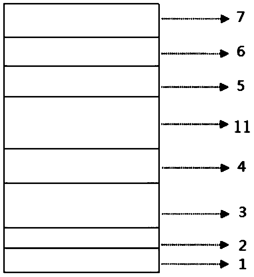
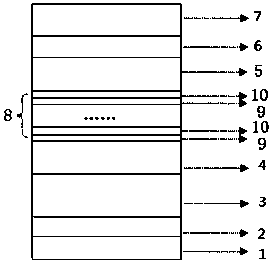
[0077] The invention uses Veeco MOCVD to grow high-brightness GaN-based LED epitaxial wafers. Using high-purity H 2 or high purity N 2 or high purity H 2 and high purity N 2 The mixed gas as the carrier gas, high-purity NH 3 As N source, trimethylgallium (TMGa) and triethylgallium (TEGa) as gallium source, trimethylindium (TMIn) as indium source, silane (SiH4) as N-type dopant, trimethylaluminum ( TMAl) as the aluminum source, magnesocene (CP2Mg) as the P-type dopant, the substrate is (0001) plane sapphire, and the reaction chamber pressure is between 100torr and 600torr. The specific growth method is as follows (for the epitaxial structure, see figure 2 , please refer to the energy band of the electron blocking layer in step 5 Figure 4 ):

[0078] 1. Under the hydrogen atmosphere of 1000-1100℃, the pressure of the reaction chamber is controlled at 200-500torr, and the sapphire substrate is treated at high temperature for 5-6min; then the temperature is lowered to 530...


PUM


Abstract

The invention provides an epitaxial growth method for blocking electron leakage and defect extension. The method comprises letting NH3, TMGa and TMAl in between a growth multi-quantum well InxGa(1-x)N/GaN layer and a growth P-type GaN layer, and growing an electron barrier layer with a growth thickness of 8 to 25 nm, wherein the layer comprises two to six groups of double-layer structures, and compared to the Al component content of the UAlGaN layer of the last double-layer structure, the Al component content of the UAlGaN layer of each double-structure is increased by 15% to 50%. According to the invention, the UAlGaN/UGaN structure with layer-to-layer gradually increased Al components is utilized as an electron barrier layer, the single energy level height distribution of a conventional P-spacer energy band is changed, the blocking effects on cavity injection are weakened, and the MQW luminescence efficiency is improved.

Description

technical field [0001] The invention relates to the technical field of LED epitaxial design, in particular to an epitaxial growth method and structure for blocking electron leakage and defect extension. Background technique [0002] GaN-based light-emitting diodes (LEDs) have been widely used in traffic lights, outdoor full-color displays, urban landscape lighting, automotive interior and exterior lights, and tunnel lights. Large-size high-power chip specifications such as 30mil*30mil, 45mil*45mil, 50mil*50mil, etc. are mostly used for lighting. The key technology of large-size chips no longer defines the luminous performance of large-size chips by high lumens, but uses lumens / watt (ie, light efficiency) as an important indicator to measure high-power light-emitting devices. [0003] At present, most innovations to improve large-scale light efficiency lie in the improvement of the quantum well layer and the P-type layer, such as reducing the energy band distortion of the qu...

Claims


Application Information

Patent Timeline
Patent Type & Authority Applications(China)
IPC IPC(8): H01L33/14H01L33/00
CPCH01L33/0075H01L33/06H01L33/145
Inventor 从颖姚振苗振林牛凤娟
Owner XIANGNENG HUALEI OPTOELECTRONICS
Why Eureka
Try Eureka