Infrared detector of microbridge structure and method for manufacturing same

A technology of infrared detector and micro-bridge structure, applied in the field of micro-electromechanical, can solve the problems of affecting the resonance effect of infrared incident light waves, reducing infrared absorption efficiency, etc., so as to improve thermal isolation effect and response rate, optimize device performance, and increase design space. Effect

Active Publication Date: 2014-04-30
ZHEJIANG DALI TECH
View PDF7 Cites 54 Cited by
  • Summary
  • Abstract
  • Description
  • Claims
  • Application Information

AI Technical Summary

Problems solved by technology

The focus of the double-layer structure design is to completely separate the infrared reflection layer 21 from the plane where the heat-insulating bridge legs 23 are located, so that they no longer affect each other, but this structure also has defects, that is, the large-area infrared absorption layer 25 and the infrared reflection layer The bridge leg 23 is sandwiched in the resonant cavity 24 formed by 21, and the bridge leg 23 will affect the resonance effect of the infrared incident light wave and reduce the infrared absorption efficiency

Method used


Image

  • Infrared detector of microbridge structure and method for manufacturing same
  • Infrared detector of microbridge structure and method for manufacturing same
  • Infrared detector of microbridge structure and method for manufacturing same

Examples


Embodiment Construction

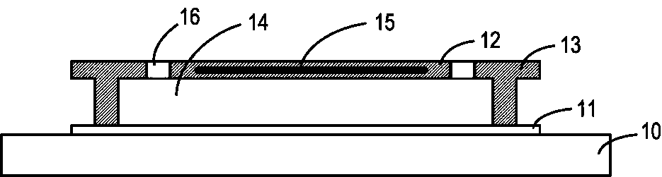
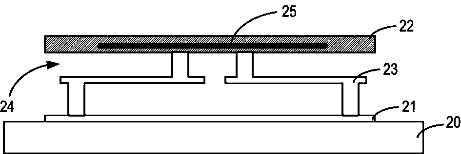
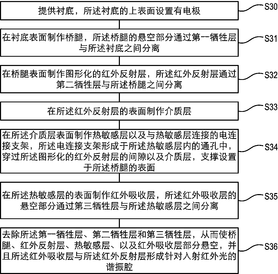
[0026] The specific implementation of the infrared detector with microbridge structure and its manufacturing method provided by the present invention will be described in detail below in conjunction with the accompanying drawings.

[0027] attached image 3 Shown is a schematic diagram of the manufacturing process of the microbridge infrared detector according to the specific embodiment of the present invention, including: step S30, providing a substrate, the upper surface of the substrate is provided with electrodes; step S31, making bridge legs on the substrate surface , the suspended part of the bridge leg is separated from the substrate through the first sacrificial layer; step S32, making a patterned infrared reflective layer on the surface of the bridge leg, and the infrared reflective layer is separated from the substrate through the second sacrificial layer Separation between the bridge legs; Step S33, making a dielectric layer on the surface of the infrared reflection...


PUM


Abstract

The invention provides an infrared detector of a microbridge structure and a method for manufacturing the infrared detector of the microbridge structure. The detector comprises a reading circuit substrate, a microbridge leg, a heat sensitive layer, an infrared reflection layer and an infrared absorption layer. The infrared absorption layer is supported by and arranged above the heat sensitive layer, a resonant cavity for incoming infrared light is formed by the infrared absorption layer and the infrared reflection layer, and the microbridge leg is arranged below the infrared reflection layer and electrically connected with the reading circuit substrate. Through the structure, the infrared absorptivity of the device can be improved while thermal conductance of the device can be reduced, the filling rate of the device is improved, the defects of the resonant cavity are overcome, and thus the thermal isolation effect and the responsivity of the device are improved and the performance of the device is optimized.

Description

technical field [0001] The invention belongs to the field of micro-electromechanical technology, and in particular relates to a multi-layer micro-bridge structure infrared detector and a manufacturing method thereof. Background technique [0002] Infrared detectors in the prior art use a MEMS microbridge structure integrated on a CMOS circuit, and use a sensitive material detection layer (usually amorphous silicon or vanadium oxide) to absorb infrared rays and convert them into electrical signals, thereby realizing thermal Imaging function. At present, the main development direction of infrared detectors is to reduce the size of the pixel structure and increase the size of the array, improve the image resolution of the detector, and expand the application range of infrared detectors. The level of its MEMS manufacturing process has become the main factor restricting product performance. factor. The microbridge structure of the infrared detector has shrunk from the early 100...

Claims


Application Information

Patent Timeline
Patent Type & Authority Applications(China)
IPC IPC(8): G01J5/10B81B7/02B81C1/00
Inventor 钱良山孟如男王景道池积光姜利军
Owner ZHEJIANG DALI TECH
Why Eureka
Try Eureka