

Etching method of etching hole having inclined side wall
A technology of sloping sidewalls and etching holes, applied in the field of plasma processing, can solve the problems of difficult control, reduced processing efficiency, poor sidewall smoothness, etc., and achieves the effect of simple control method and fast etching rate
- Summary
- Abstract
- Description
- Claims
- Application Information
AI Technical Summary
Problems solved by technology
Method used
Image

Examples
Embodiment Construction
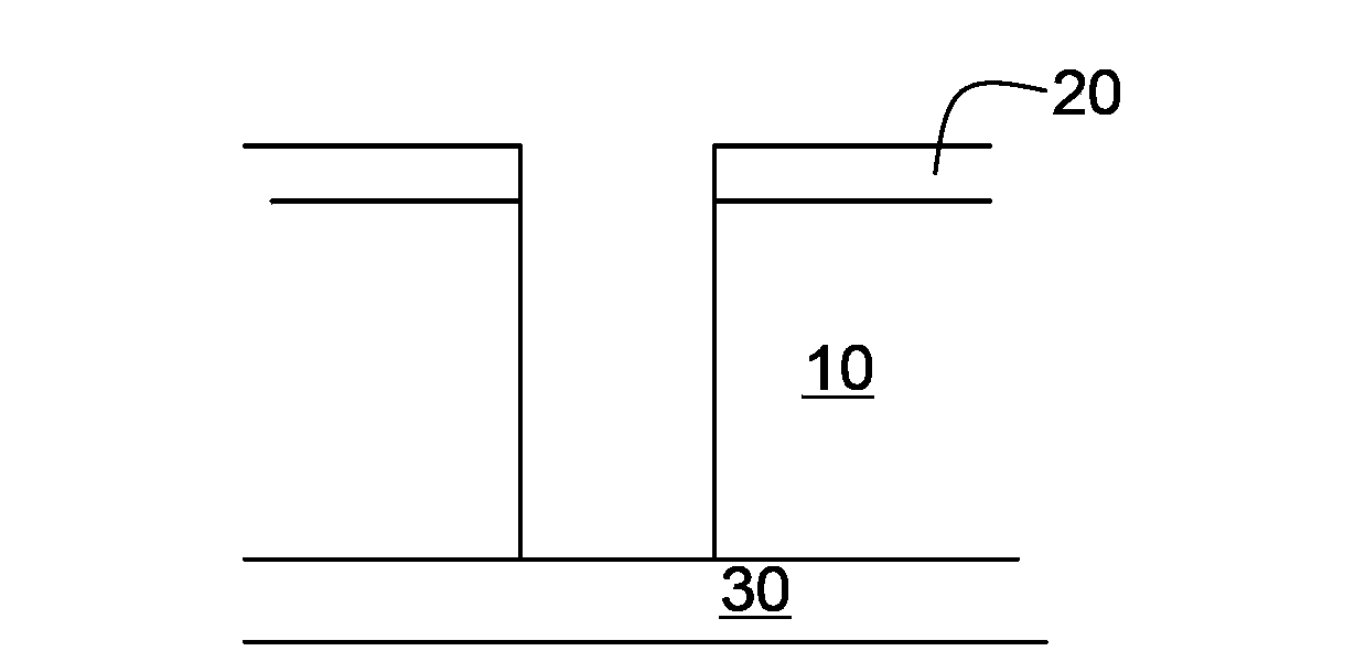
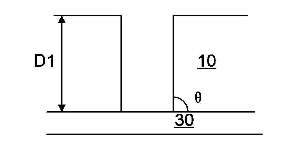
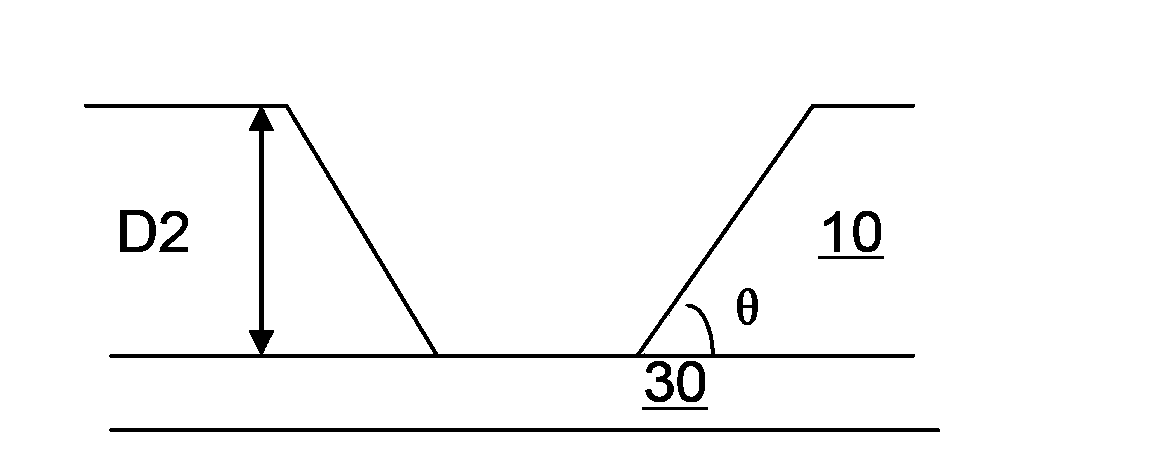
[0018] Combine the following Figure 1a ~c, the present invention is explained in detail through preferred specific embodiments.
[0019] Compared with the prior art that completes the downward etching and sidewall topography control at one time, the present invention adopts a step-by-step method to complete the downward etching and sidewall topography modification respectively. Such as Figure 1a Shown is the overall schematic diagram of the deep silicon etching hole forming the straight hole in the first step of the etching method of the present invention. The etching target layer 20 of the present invention is a crystalline silicon layer, and above the silicon layer is a mask layer 20. The mask layer may be a traditional photoresist (PR) material or a mask layer of other organic materials. Below the crystalline silicon layer 10 is an etch stop layer 30. The etch stop layer may be a material layer different from the silicon material, such as SiO2, SiN, or a colloid made of organ...
PUM
 Abstract
Description
Claims
Application Information