

Resistive random access memory structure and preparation method thereof
A technology of resistive variable memory and resistive variable layer, which is applied in the direction of static memory, digital memory information, information storage, etc., can solve the problems of device switching ratio reduction, complex process, low repeatability, etc., and reduce power consumption when turning on and off , good mechanical stability, low power consumption
- Summary
- Abstract
- Description
- Claims
- Application Information
AI Technical Summary
Problems solved by technology
Method used
Image

Examples
Embodiment 1
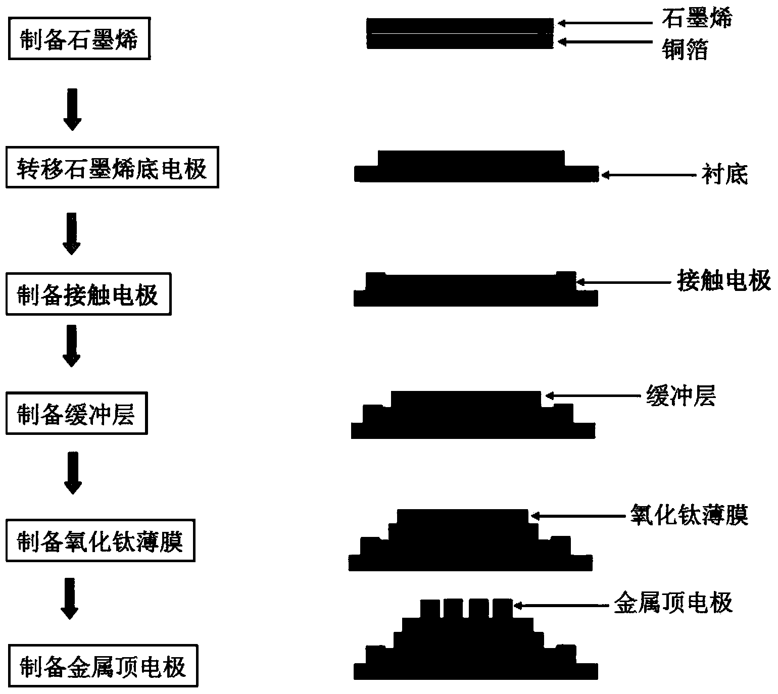
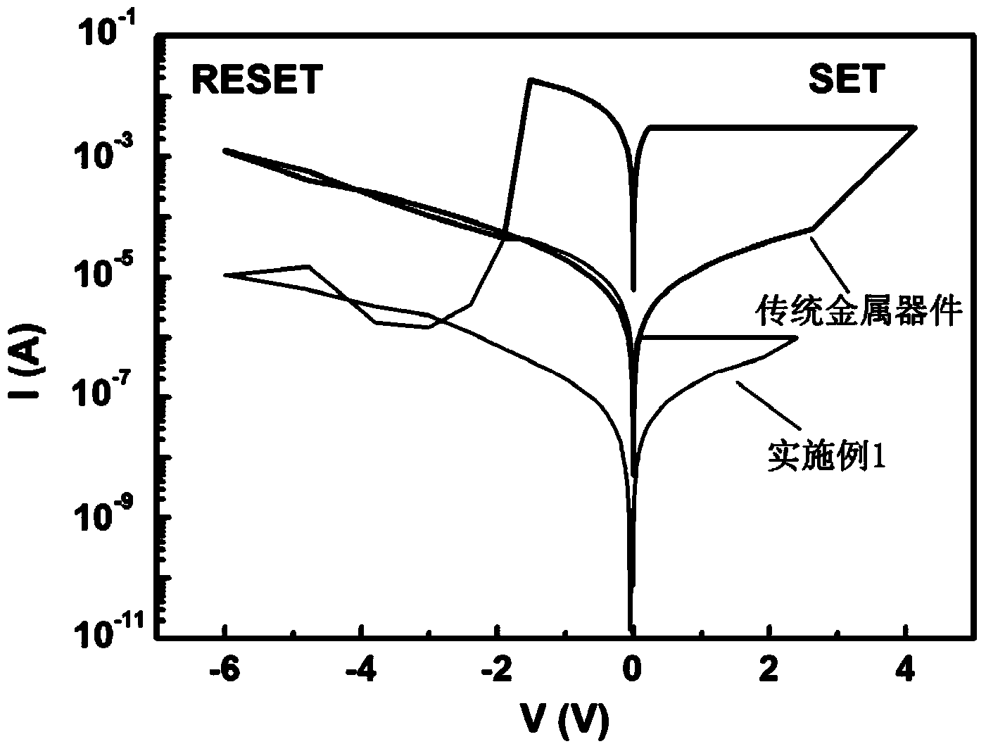
[0048] This embodiment provides an ultra-low power consumption resistive memory structure, which is prepared through the following steps (the specific preparation process is as follows: figure 1 shown):
[0049] 1. Preparation / transfer of graphene
[0050] Graphene is prepared on the surface of copper foil by chemical vapor deposition method, the temperature is 1050 °C, the gas is 4 sccm of methane and 200 sccm of hydrogen, and the vacuum is 200 Torr; after the growth of graphene is completed, spin-coat PMMA on the graphene / copper foil The surface of the graphene is etched with ferric chloride solution to remove the copper foil, and the remaining PMMA / graphene is transferred to the silicon wafer substrate, and the PMMA is dissolved with acetone, leaving a composite of graphene and the substrate. The thickness of graphene is 0.34nm;
[0051] After transfer to the target substrate, metal electrodes (contact electrodes) were prepared on both ends of the graphene as the bottom e...
Embodiment 2
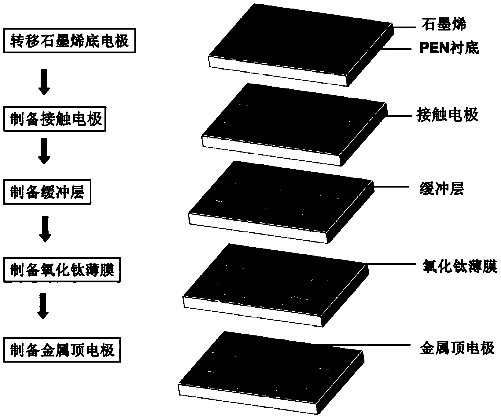
[0060] This embodiment provides a flexible and transparent resistive memory with ultra-low power consumption, which is prepared by the following steps (the specific preparation process is as follows: image 3 shown):
[0061] 1. Preparation / transfer of graphene
[0062] Graphene is prepared on the surface of copper foil by chemical vapor deposition method, the temperature is 1050 °C, the gas is 4 sccm of methane and 200 sccm of hydrogen, and the vacuum is 200 Torr; after the growth of graphene is completed, spin-coat PMMA on the graphene / copper foil The surface of the graphene is etched with a ferric chloride solution to remove the copper foil, and the remaining PMMA / graphene is transferred to the PEN flexible substrate, and the PMMA is dissolved with acetone, leaving a composite of graphene and the substrate;
[0063] After being transferred to the target substrate, a metal mask plate with a width of 200 μm is placed on the graphene, and a graphene strip with a width of 200 ...
PUM
| Property | Measurement | Unit |
|---|---|---|
| Thickness | aaaaa | aaaaa |
| Thickness | aaaaa | aaaaa |
| Thickness | aaaaa | aaaaa |
Abstract
Description
Claims
Application Information