Grapheme silicon-based solar cell and manufacture method thereof
A technology of solar cells and graphene, which is applied in the direction of final product manufacturing, sustainable manufacturing/processing, circuits, etc., can solve the problem of low photoelectric conversion efficiency of solar cells, achieve the effect of improving battery conversion efficiency, improving efficiency, and solving the problem of reducing
- Summary
- Abstract
- Description
- Claims
- Application Information
AI Technical Summary
Problems solved by technology
Method used
Image
Examples
Embodiment 1
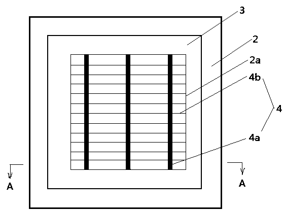
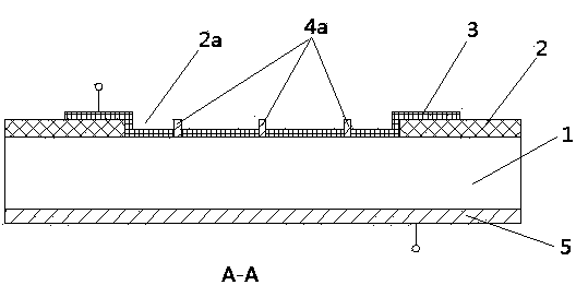
[0026] See figure 1 and figure 2 , to prepare silicon dioxide SiO on the front surface of n-type single crystal silicon wafer 2 layer, silicon dioxide SiO 2 There are through holes in the layer; the grid electrode structure is as follows figure 1 As shown, there are multiple main grid electrodes in the vertical direction, and auxiliary grid electrodes are arranged in the horizontal direction. The main grid electrodes and the auxiliary grid electrodes are arranged in a grid pattern. Apply photosensitive glue on the screen, and write the electrode structure on the screen through photolithography; use a screen printing machine to print Ag paste on the n-type monocrystalline silicon exposed by the through hole of the silicon dioxide layer according to the image on the screen On the chip, the Ag electrode is sintered at high temperature; the graphene solution is spread on the surface of the silicon dioxide layer and the n-type single crystal silicon chip exposed by the through ...
Embodiment 2
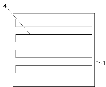
[0028] Please refer to Example 1 and see image 3 , to prepare silicon dioxide SiO on the front surface of n-type single crystal silicon wafer 2 layer, silicon dioxide SiO 2 There are through holes in the layer; the graphene solution is spread on the surface of the silicon dioxide layer and the n-type single crystal silicon wafer exposed by the through holes of the silicon dioxide layer by spraying process, and the graphene film and the n-type single crystal silicon Sheet bonding; grid electrode structure such as image 3 As shown, it is an S-shaped arrangement of a single grid line electrode. The structure of the grid line electrode is drawn on the screen, and photosensitive glue is coated on the screen, and the electrode structure is drawn on the screen through a photolithography process; use a screen printing machine Print the Ag paste on the graphene film in the through-hole part of the silicon dioxide layer according to the image on the screen plate, and sinter at high ...
Embodiment 3
[0037] Please refer to Example 1 and see Figure 5 , to prepare silicon dioxide SiO on the front surface of n-type single crystal silicon wafer 2 layer, silicon dioxide SiO 2 There are through holes in the layer; the grid electrode structure is as follows Figure 5 As shown, in silica SiO 2In the through hole area, the main grid electrode divides the surface of the n-type single crystal silicon wafer into several sub grid electrode areas. The sub grid electrode is arranged in the sub grid electrode area and connected to the main grid electrode. The included angle α with the main grid line electrode is 30°~80°, and the sub-grid line electrodes in the adjacent sub-grid line electrode areas are arranged symmetrically with respect to the main grid line electrodes that divide the adjacent sub-grid line electrode areas; The wire electrode structure is drawn on the screen, and the photosensitive glue is coated on the screen, and the electrode structure is drawn on the screen throu...
PUM
 Abstract
Description
Claims
Application Information


