Transparent conductive film and preparation method thereof
A technology of transparent conductive film and conductive material, applied in chemical instruments and methods, synthetic resin layered products, lamination devices, etc., to achieve the effects of good uniformity, uniform thickness and strong applicability
- Summary
- Abstract
- Description
- Claims
- Application Information
AI Technical Summary
Problems solved by technology
Method used
Image
Examples
Embodiment 1
[0034] 1. Preparation of spinning solution
[0035] Add 5g of polyethylene dioxythiophene (PEDOT) with a weight average molecular weight of about 50,000 and 0.2g of polystyrene sodium sulfonate (PSS) into 100ml of pure water, stir well, then stand still until the bubbles are completely Disappeared, the spinning solution was obtained.
[0036] 2. Preparation of nanofibers
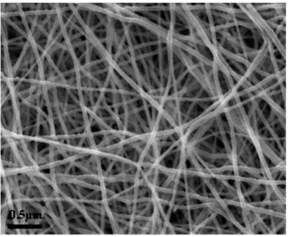
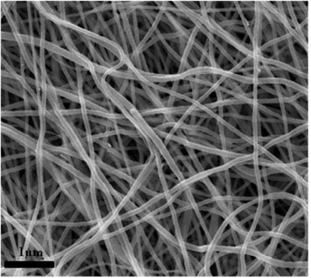
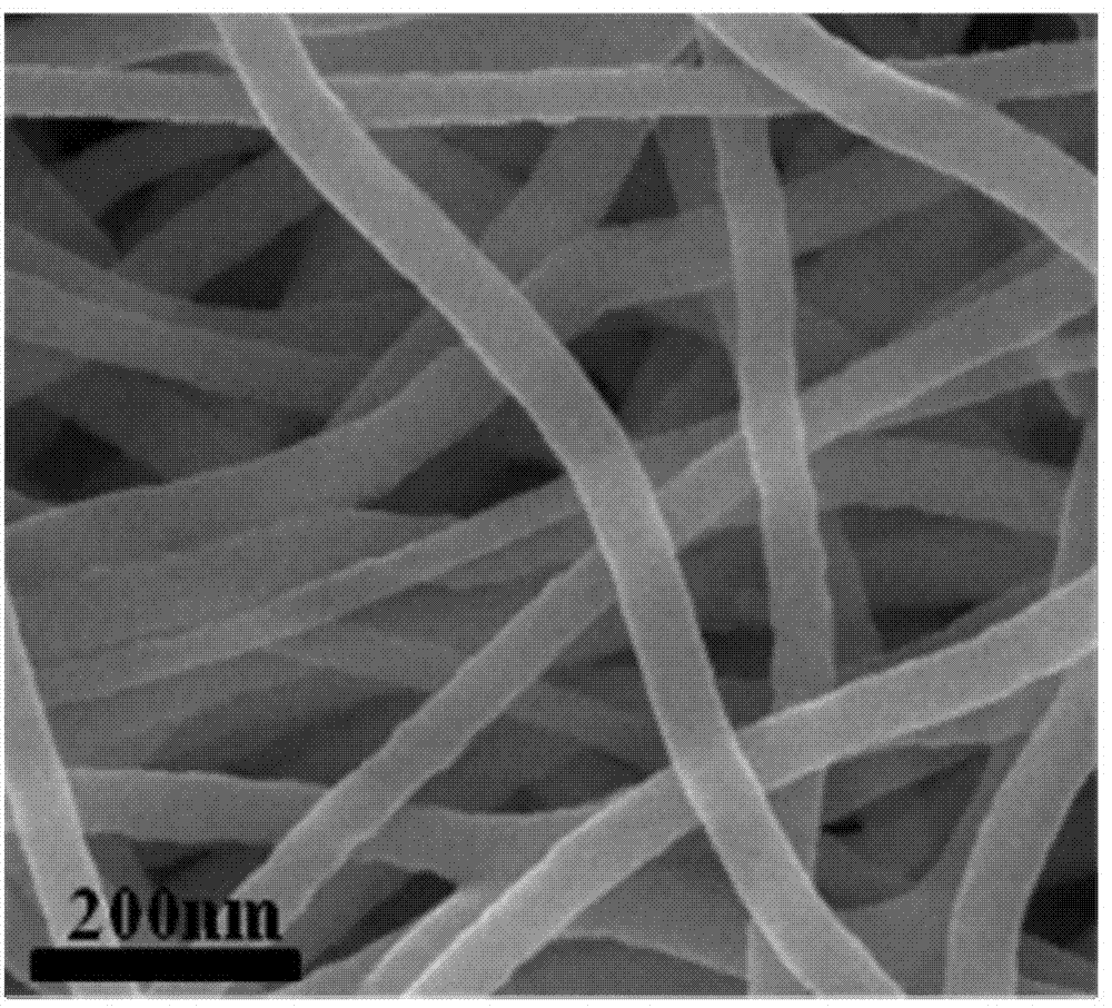
[0037] Add the above spinning solution to the feeding device of the electrospinning equipment, set the spinning voltage to 15kV, the feeding rate of the spinning solution (ie spinning rate) to 20ul / min, and the receiving distance to 8cm, using electrospinning Spray the above-mentioned spinning solution onto the inorganic glass (transparent substrate) with a thickness of 0.1 mm, so that the nano-conductive fibers formed by electrospinning are evenly deposited on the inorganic glass, and the spraying time is controlled to be 2 to 3 minutes. A conductive layer with a thickness of about 1 μm is formed on the ino...
Embodiment 2
[0040] Add 5g of polyethylenedioxythiophene with a weight-average molecular weight of about 50,000, 0.2g of sodium polystyrene sulfonate and 0.2g of graphene with a particle size of ≤20nm into 100ml of pure water, stir well, and let it stand still , when the air bubbles completely disappeared, the spinning solution was obtained.
[0041] Using the method described in Example 1, the above-mentioned spinning solution is sprayed onto an inorganic glass with a thickness of 0.1 mm to form a conductive layer with a thickness of about 1 μm, that is, a transparent conductive film is obtained, which includes an inorganic glass substrate and is located on the inorganic glass. The conductive layer on the substrate is formed by uniformly and interlacedly depositing nano-conductive fibers with uniform size, good shape, and evenly dispersed graphene on the inorganic glass.
Embodiment 3
[0043] 1. Preparation of spinning solution
[0044] Add 10g of polyethylenedioxythiophene with a weight-average molecular weight of about 30,000 and 0.1g of sodium polystyrene sulfonate into 100ml of pure water, stir thoroughly, and then stand still until the bubbles completely disappear to obtain spinning liquid.
[0045] 2. Preparation of nanofibers
[0046] The above-mentioned spinning solution is added to the feeding device of the electrospinning equipment, the spinning voltage is set to 40kV, the feeding rate of the spinning solution is 30ul / min, the receiving distance is 20cm, and the above-mentioned spinning solution is obtained by electrospinning. Spray onto a PET transparent substrate with a thickness of 0.2mm, so that the nano-conductive fibers formed by electrospinning are evenly and interlacedly deposited on the transparent substrate, and the amount of spinning solution is controlled to make the nano-conductive fibers on the transparent substrate A conductive lay...
PUM
| Property | Measurement | Unit |
|---|---|---|
| thickness | aaaaa | aaaaa |
| particle diameter | aaaaa | aaaaa |
| particle diameter | aaaaa | aaaaa |
Abstract
Description
Claims
Application Information


