

Method for manufacturing ultrahigh-density germanium silicon quantum dots based on obliquely-cut silicon substrate
A technology of ultra-high density and quantum dots, which is applied in the field of preparing high-quality ultra-high-density germanium-silicon quantum dots. It can solve the problems of high-density quantum dot materials such as cumbersome process and low quality, and achieve the improvement of photoelectric conversion efficiency. The method is simple and easy , the effect of inhibiting surface migration
- Summary
- Abstract
- Description
- Claims
- Application Information
AI Technical Summary
Problems solved by technology
Method used
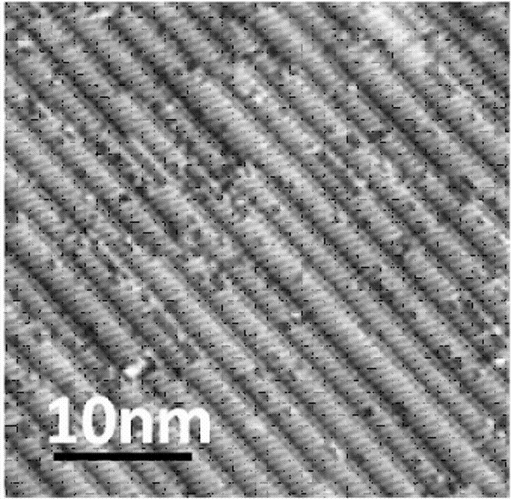
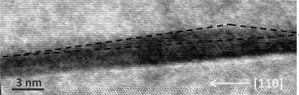
Image

Examples
Embodiment 1
[0023] The chamfered silicon-based substrate needs to be cleaned before being put into the molecular beam epitaxy equipment for growth. The cleaning procedure is as follows:
[0024] (1) Sonicate the beveled Si(100) single wafer in acetone and methanol for 5 minutes each to remove organic matter on the substrate surface. Sonicate in deionized water for 5 minutes;
[0025] (2) After soaking in a mixed solution of sulfuric acid and hydrogen peroxide (volume ratio 4:1) for 10 minutes, rinse with deionized water for 10 minutes;
[0026] (3) After 15 minutes in a water bath at 80°C in a mixed solution of ammonia, hydrogen peroxide, and water (volume ratio 1:1:5), rinse with deionized water for 15 minutes;
[0027] (4) After bathing in a mixed solution of hydrochloric acid, hydrogen peroxide, and water (volume ratio 1:1:5) at 80°C for 15 minutes, rinse with deionized water for 15 minutes;
[0028] (5) Soak in 5wt% hydrofluoric acid for 60-80 seconds to remove the oxide layer on t...
Embodiment 2
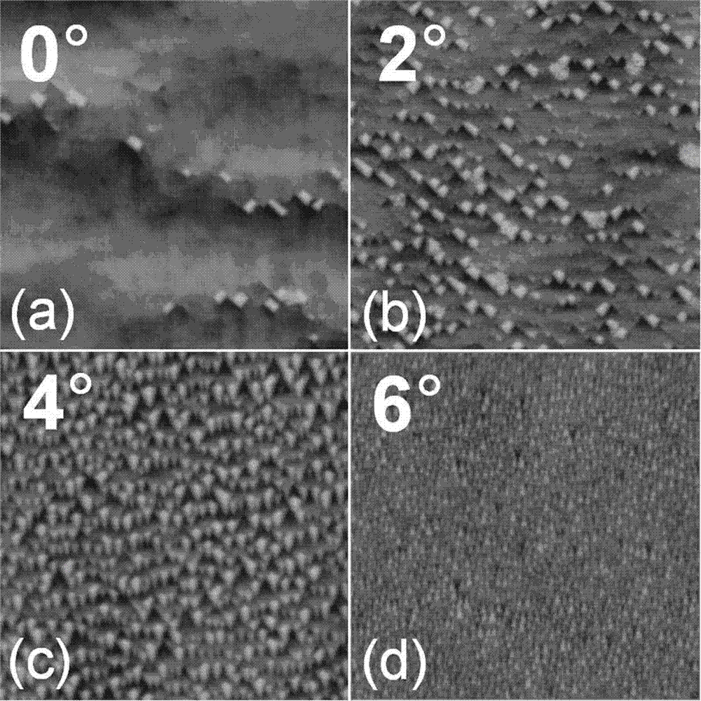
[0030] Take the n-type silicon single wafer whose bevel direction is the direction and whose bevel angle is 2°, after cleaning according to the cleaning procedure described in Example 1, put it into molecular beam epitaxy equipment to carry out molecular beam epitaxy of germanium nanomaterials grow. The sampling chamber and the growth chamber were maintained at (10 -8 -10 -10 ) torr vacuum. Both silicon and germanium sources of the system are evaporated by electron beam heating. The following are the process conditions for material growth.
[0031] i) Heating the substrate to 1000°C for 5 minutes to desorb the impurity atoms on the surface;
[0032] ii) Lower the substrate temperature to grow a silicon buffer layer, the buffer layer growth temperature: 500°C, growth thickness: 50nm. Growth rate 0.6? / s;
[0033] iii) Epitaxial growth of silicon-germanium nanomaterials, growth temperature: 400°C, growth rate 0.05 ? / s, thickness of germanium growth 1.2nm, growth rate thick...
Embodiment 3
[0038] Take the p-type silicon single wafer whose bevel direction is the direction and whose bevel angle is 4°, after cleaning according to the cleaning procedure described in Example 1, put it into molecular beam epitaxy equipment for molecular beam epitaxy of germanium nanomaterials grow. The sampling chamber and the growth chamber were maintained at (10 -8 -10 -10 ) torr vacuum. Both silicon and germanium sources of the system are evaporated by electron beam heating. The following are the process conditions for material growth.
[0039] i) Heating the substrate to 800°C for 15 minutes to desorb the impurity atoms on the surface;
[0040] ii) Lower the substrate temperature to grow a silicon buffer layer, the buffer layer growth temperature: 600°C, growth thickness: 100nm. Growth rate 0.6 ? / s;
[0041] iii) Epitaxial growth of germanium silicon nanomaterials, growth temperature: 600°C, growth rate 0.05 ? / s, thickness of germanium growth 0.9nm, immediately lower the te...
PUM
| Property | Measurement | Unit |
|---|---|---|
| Diameter | aaaaa | aaaaa |
| Diameter | aaaaa | aaaaa |
| Diameter | aaaaa | aaaaa |
Abstract
Description
Claims
Application Information