Oxide semiconductor manufacturing method

A technology of oxide semiconductors and manufacturing methods, applied in semiconductor/solid-state device manufacturing, semiconductor devices, transistors, etc., can solve problems such as uncontrollable or adjustment, and affect the manufacturing quality of thin-film transistors, and achieve the effect of improving manufacturing quality

Active Publication Date: 2017-03-08
上海鸿隽电子科技有限公司
View PDF3 Cites 0 Cited by
  • Summary
  • Abstract
  • Description
  • Claims
  • Application Information

AI Technical Summary

Problems solved by technology

[0003] In the traditional thin film transistor manufacturing method, the channel layer (active layer, i.e. channel layer) is an indium gallium zinc oxide (IGZO) film deposited by a single target material, and the material of the target material is usually InGaZnO 4 、In 2 Ga 2 ZnO 7 、In 2 o 3 (ZnO) m (m=2~20), etc. However, the composition ratio of the channel layer film manufactured by this traditional manufacturing method is directly determined by the material composition of the target, and cannot be controlled or adjusted during the deposition process, thus affecting the thin film transistor. manufacturing quality

Method used


Image

  • Oxide semiconductor manufacturing method
  • Oxide semiconductor manufacturing method
  • Oxide semiconductor manufacturing method

Examples


Embodiment Construction

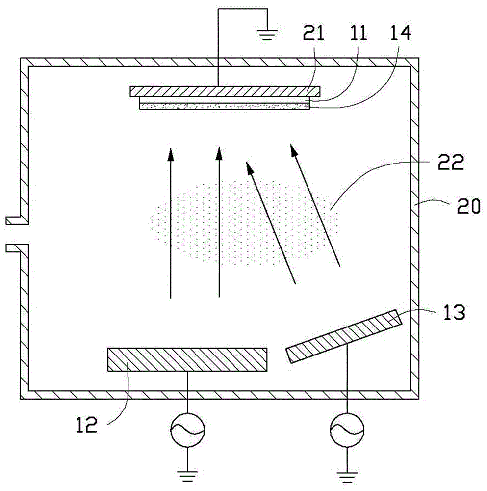
[0027] see figure 1 , the first embodiment of the present invention provides a method for manufacturing an oxide semiconductor, the steps of which are specifically described as follows.

[0028] First, a substrate 11 is provided. The substrate 11 is used to carry the subsequently formed oxide semiconductor thin film. The substrate 11 can be glass, quartz, silicon wafer, plastic and so on.

[0029] Secondly, metal ions from the first metal oxide target 12 are sputtered on the substrate 11, and at least two metal ions from the second metal oxide target 13 are sputtered on the substrate 11 to deposit and form oxides Semiconductor film 14. The at least two metal ions on the second metal oxide target are different from the metal ions on the first metal oxide target. When depositing metal ions, the composition ratio of the oxide semiconductor film 14 can be adjusted by controlling the deposition rate of the oxide semiconductor film 14 and the service period of the baffle of the ...


PUM


Abstract

The invention provides an oxide semiconductor manufacturing method comprising that a substrate is provided. Metal ions from a first metal oxide target material are sputtering-coated on the substrate and at least two types of metal ions from a second metal oxide target material are sputtering-coated on the substrate so that an oxide semiconductor thin film is formed via deposition. In the sputtering-coating process, thin film deposition rate and use cycle of a sputtering-coating device blocking plate are controlled so that composition proportion of the thin film is adjusted. The at least two types of metal ions on the second metal oxide target material are different from the metal irons from the first metal oxide target material. Composition proportion of the prepared oxide semiconductor thin film can be effectively controlled by the method so that enhancement of manufacturing quality of a thin-film transistor is facilitated. The invention also provides a thin-film transistor manufacturing method.

Description

technical field [0001] The present invention relates to a method for manufacturing an oxide semiconductor. Background technique [0002] With the advancement of process technology, thin film transistors have been widely used in displays to meet the requirements of thinning and miniaturization of displays. Thin film transistors generally include components such as gate, drain, source, and channel layer, which change the conductivity of the channel layer by controlling the voltage of the gate, so that the source and drain are turned on or off. state. [0003] In the traditional thin film transistor manufacturing method, the channel layer (active layer, i.e. channel layer) is an indium gallium zinc oxide (IGZO) film deposited by a single target material, and the material of the target material is usually InGaZnO 4 、In 2 Ga 2 ZnO 7 、In 2 o 3 (ZnO) m (m=2~20), etc. However, the composition ratio of the channel layer film manufactured by this traditional manufacturing meth...

Claims


Application Information

Patent Timeline
Patent Type & Authority Patents(China)
IPC IPC(8): H01L21/363C23C14/34C23C14/08H01L29/786
CPCC23C14/08C23C14/28C23C14/3464C23C16/40C23C16/45525H01L21/02565H01L21/02631H01L29/7869
Inventor 王良源
Owner 上海鸿隽电子科技有限公司
Why Eureka
Try Eureka