

Manufacturing process of low dielectric constant film layer for microelectronic chip
A technology with low dielectric constant and manufacturing process, which is applied in metal material coating process, semiconductor/solid-state device manufacturing, coating, etc., can solve the problems of unsuitable insulating materials and high dielectric constant value of insulating materials, and achieve convenient and accurate Controlling, good uniformity and reliability, effect of uniform chemical composition
- Summary
- Abstract
- Description
- Claims
- Application Information
AI Technical Summary
Problems solved by technology
Method used
Image

Examples
Embodiment 1~7
[0019] Embodiment 1~7: a kind of manufacturing process of low dielectric constant thin film layer for microelectronic chip, it is characterized in that: described manufacturing process is based on a deposition device, and this deposition device comprises furnace body, respectively is positioned at furnace body both sides resistant A stainless steel kettle and a vacuum pump, the first half of the furnace body is wound with an induction coil, and the induction coil is connected to a 13.36MHz radio frequency power supply and a matching device in turn, and the second half of the furnace body is a heating temperature zone; including the following steps:
[0020] Step 1. Exhaust the gas in the furnace to form a gas that is less than 10 -3 Pa vacuum condition, start 13.36MHz RF power supply and matcher;
[0021] Step 2. Inject tetraethyl orthosilicate into the pressure-resistant stainless steel kettle, which is sealed with one end of the furnace body through a pipeline, and nitrogen ...
Embodiment 1
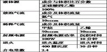
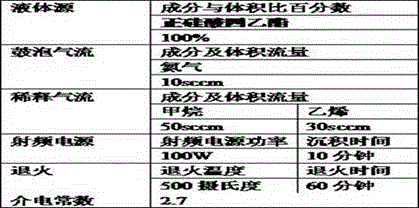
[0027]
Embodiment 2
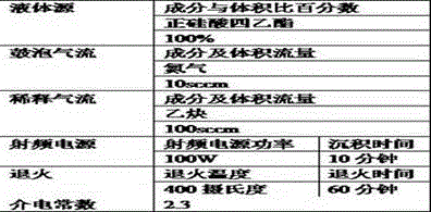
[0029]
PUM
 Abstract
Description
Claims
Application Information