

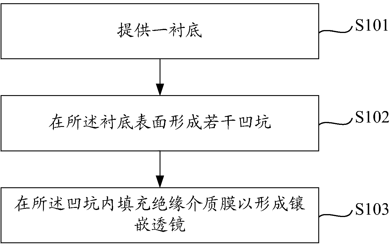
Graphical substrate and inverted LED chip and manufacturing method thereof
A patterned substrate, LED chip technology, applied in the direction of electrical components, circuits, semiconductor devices, etc., can solve the problems of reducing chip life, reducing chip light output, increasing chip voltage, etc., to achieve the effect of improving light output efficiency and reducing light reflection
- Summary
- Abstract
- Description
- Claims
- Application Information
AI Technical Summary
Problems solved by technology
Method used
Image

Examples
Embodiment 1
[0055] Figure 2a ~ 2gIt is a cross-sectional view of structures in each step of the method for manufacturing a patterned substrate according to Embodiment 1 of the present invention.
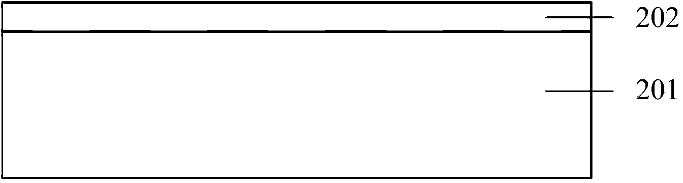
[0056] Such as Figure 2a As shown, a substrate 201 having a first side and a second side is provided. The substrate 201 is made of a light-transmitting material, for example, it can be sapphire, silicon carbide (SiC), zinc oxide (ZnO), spinel (MgAL 2 o 4 ). In this embodiment, the substrate 201 is a sapphire substrate.
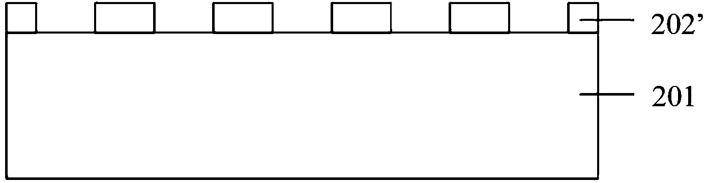
[0057] continue to refer Figure 2a , forming a hard mask layer 202 on the first surface of the substrate 201 . The hard mask layer 202 is preferably silicon dioxide (SiO2). The silicon dioxide may be formed by chemical vapor deposition (CVD), such as plasma enhanced chemical vapor deposition (PECVD), and its thickness is, for example, 0.5-10 μm. The hard mask layer is used as a mask for the subsequent process of forming pits, so its thickness depends on the size of th...
Embodiment 2
[0074] Figure 3a-3e It is a cross-sectional view of the structure in each step of the patterned substrate manufacturing method according to the second embodiment of the present invention.
[0075] Such as Figure 3a As shown, a substrate 301 is provided. The substrate 301 is made of a light-transmitting material, for example, it can be sapphire, silicon carbide (SiC), zinc oxide (ZnO), spinel (MgAL 2 o 4 ). In this embodiment, the substrate 301 is a sapphire substrate.
[0076] continue to refer Figure 3a , forming a photoresist 303 on the surface of the substrate 301 . The thickness of the photoresist is, for example, 1-2 μm.
[0077] refer to Figure 3b , a patterned photoresist can be formed through coating, exposure and development processes. The patterned photoresist includes a plurality of cylindrical photoresist stages, the cylindrical photoresist stage means that the photoresist stage is circular when viewed from above (parallel to the surface direction of t...
PUM
| Property | Measurement | Unit |
|---|---|---|
| thickness | aaaaa | aaaaa |
| depth | aaaaa | aaaaa |
| depth | aaaaa | aaaaa |
Abstract
Description
Claims
Application Information