Preparation method of cadmium arsenide semiconductor nanocluster

A technology of nanoclusters and semiconductors, which is applied in the field of synthesis of a large number of cadmium arsenide nanoclusters, which can solve the problems of few cadmium arsenide nanoclusters, difficult storage, cumbersome methods, etc., and achieve good monodispersity, good luminescent properties, and reaction Simple operation effect

Inactive Publication Date: 2014-07-23
JILIN UNIV
View PDF2 Cites 6 Cited by
  • Summary
  • Abstract
  • Description
  • Claims
  • Application Information

AI Technical Summary

Problems solved by technology

At present, the synthesis methods of magic-sized nanoclusters are relatively cumbersome, using a large amount of phosphorus-containing compounds, and the optical properties are not very good, and the fluorescence quantum efficiency is low.
[0005] CdAs nanoclusters are typical II-V semiconductor nanoclusters. Compared with common II-VI (such as CdSe, CdS, etc.) The method is relatively cumbersome, the synthesis process is limited by materials, the cost is expensive, and it is not conducive to large-scale synthesis. For example, the Bawendi group reported in 2011 using very active 3-(trimethylsilyl)arsenic TMS-As as an arsenic source to prepare Cd 3 As 2 Nanoclusters (J Am.Chem.Soc.2011, 133, 4676), the TMS-As used in it is very active and prone to redox reactions. It is highly toxic, flammable and explosive, so it needs strict storage with tools such as glove boxes. Therefore, the experimental operation is relatively complicated and requires certain laboratory conditions.
In summary, the current Cd 3 As 2 There are still many problems in the synthesis of nanoclusters. Most of the existing synthesis methods require harsh experimental conditions, such as complicated and cumbersome operation processes, expensive, difficult to store and highly toxic experimental raw materials, etc.

Method used


Image

  • Preparation method of cadmium arsenide semiconductor nanocluster
  • Preparation method of cadmium arsenide semiconductor nanocluster

Examples


Embodiment 1

[0022] First, prepare the cadmium oleate solution. Take 12mmol (1.536g) of cadmium oxide powder, 25mmol (8.75mL) of OA (oleic acid) and 11.25mL of ODE (octadecene) and mix, heat to 250 ℃ under nitrogen protection to dissolve cadmium oxide, and cool to 120 ℃, prepared into cadmium oleate solution, a light yellow transparent solution.

[0023] Then take 1mmol (0.2228g) of magnesium arsenide into the reaction flask, and inject 1.5mL of hydrochloric acid with a concentration of 4mol / L. The gas produced by the reaction is passed into the above 120℃ cadmium oleate solution and reacted for 30 minutes to obtain Cd 3 As 2 Cluster compound.

Embodiment 2

[0025] First, prepare the cadmium myristate solution. Take 12mmol (1.536g) of cadmium oxide powder, 25mmol of myristic acid and 11.25mL of ODE (octadecene) and mix, heat to 250°C under nitrogen protection to dissolve cadmium oxide, and cool to 50°C to prepare myristic acid Cadmium solution is a colorless and transparent solution.

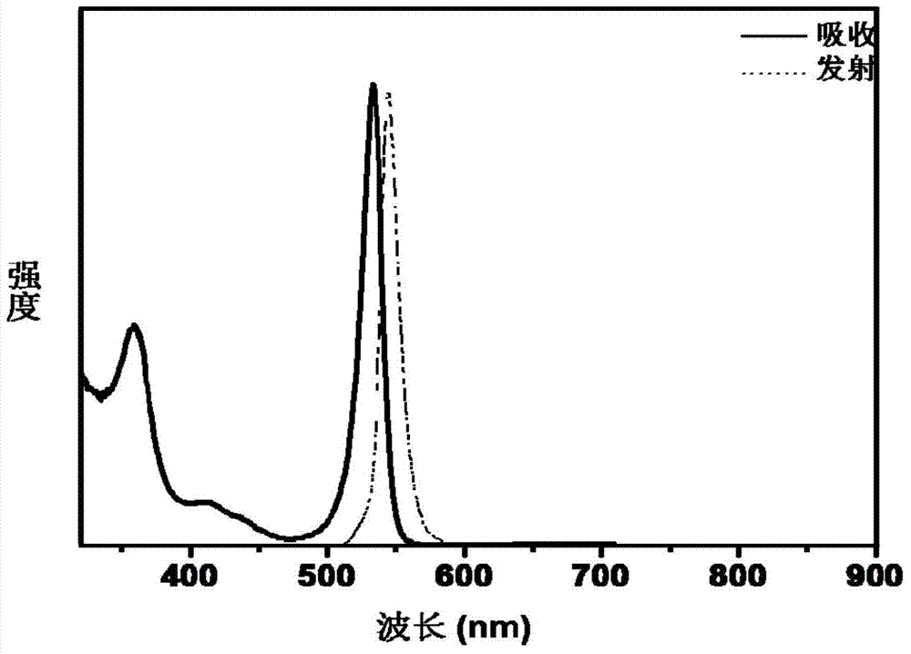
[0026] Then take 1mmol zinc arsenide into the reaction flask, and inject 1.5mL sulfuric acid with a concentration of 4mol / L. The gas produced by the reaction is passed into the above-mentioned 50℃ cadmium myristate solution and reacted for 30 minutes to obtain the Cd 3 As 2 The ultraviolet-visible absorption peaks of the cluster compounds are sharp and symmetrical, the fluorescence peaks are sharply symmetrical, and the half-peak width is very narrow, showing a good size distribution.

Embodiment 3

[0028] First, prepare the cadmium oleate solution. Take 12mmol (1.536g) of cadmium oxide powder, 25mmol of OA (oleic acid, 8.75ml) and 91.25mL of ODE (octadecene) and mix, heat to 250℃ under nitrogen protection to dissolve the cadmium oxide, and cool to 120℃ , Preparation of cadmium oleate solution, a light yellow transparent solution.

[0029] Take 2mmol of magnesium arsenide into the reaction flask, and inject 10mL of hydrochloric acid with a concentration of 4mol / L. The gas produced by the reaction is passed into the above-mentioned 120℃ cadmium oleate solution and reacted for 30 minutes to obtain Cd 3 As 2 Compared with the above-mentioned examples, the cluster compound exhibits a slightly higher concentration and more products are obtained, and the spectral effect is still symmetrical and sharp.


PUM

PropertyMeasurementUnit
refractive indexaaaaaaaaaa

Abstract

The invention relates to a preparation method of a cadmium arsenide nanocluster, particularly a synthesis method for mass preparation of a cadmium arsenide nanocluster, belonging to the technical field of preparation of semiconductor nano materials. The method comprises the following steps: reacting arsenide and inorganic acid to prepare AsH3 gas, and meanwhile, introducing the gas into a cadmium carboxylate octadecene solution under the protection of N2 to react so as to generate a Cd3As2 nanocluster compound; the nanocluster has very sharp and symmetric absorption and fluorescence peaks, and has the advantages of favorable luminescence and favorable monodispersity; the whole reaction is simple to operate; all the reactants are low in cost and easy to preserve; and the method can implement mass synthesis and does not use organic phosphorus in the reaction process.

Description

Technical field [0001] The invention belongs to the technical field of semiconductor nano material preparation, and relates to a synthetic method that can be used for mass preparation of cadmium arsenide nano clusters. Background technique [0002] After the semiconductor material gradually decreases from the bulk phase to a certain critical size (1-20 nanometers), the volatility of its carriers becomes significant, the movement will be restricted, resulting in an increase in kinetic energy, and the corresponding electronic structure is continuous from the bulk phase. The energy level structure becomes a quasi-split discontinuity, which is called the quantum size effect. The more common semiconductor nanoparticles, namely quantum dots, mainly include II-VI, III-V and IV-VI groups. These types of quantum dots all follow the quantum size effect very much, and their properties change regularly with size, for example, the absorption and emission wavelengths change with size. Theref...

Claims


Application Information

Patent Timeline
Patent Type & Authority Applications(China)
IPC IPC(8): C01G28/00B82Y30/00B82Y40/00
Inventor 解仁国李冬泽杨文胜
Owner JILIN UNIV
Why Eureka
Try Eureka