Etching liquid, etching method and surface roughening method for GaP layer of LED chip
A technology of LED chip and surface roughening, applied in electrical components, circuits, semiconductor devices, etc., can solve the problems of high cost and poor effect, and achieve the effect of easy operation, simple process and mild conditions
- Summary
- Abstract
- Description
- Claims
- Application Information
AI Technical Summary
Problems solved by technology
Method used
Image

Examples
Embodiment 1
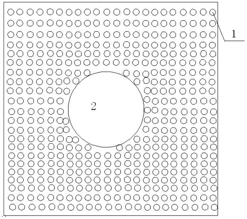
[0039] like figure 1 , figure 2 and image 3 As shown, an etching solution, an etching method and a method for roughening the surface of the GaP layer of an LED chip, the etching solution is composed of hydrochloric acid, phosphoric acid, sulfuric acid and hydrogen peroxide, and the volume fractions of each component are respectively: hydrochloric acid is 15%, phosphoric acid is 40%, sulfuric acid is 13%, hydrogen peroxide is 32%. Wherein the massfraction of hydrochloric acid is 37%, the massfraction of phosphoric acid is 20%, the massfraction of sulfuric acid is 70%, the massfraction of hydrogen peroxide is 75% the step of surface roughening of LED chip GaP layer is: (a) make mask plate, There are circular etching holes with a diameter of 5 μm and P-side electrodes on the mask plate, the distance between the etching holes is 3 μm, and the P-side electrodes are located in the center of the mask plate; (b) photolithography, using the mask plate made in step (a) Carry out ph...
Embodiment 2
[0042] Same as Example 1, the difference is that the volume fractions of the components of the etching solution are: 10% hydrochloric acid, 40% phosphoric acid, 10% sulfuric acid, 40% hydrogen peroxide, and the roughening steps of the GaP layer surface of the LED chip are the same as in Example 1 , the difference is that the flow rates of the etching gas in step (c) are respectively: wherein the volume ratio of boron trichloride, ethylene, argon and helium is 15:1:15:20, the etching time is 150s, and the etching time is 150s. Erosion depth is In step (ii), sonicate in a water bath at 45°C for 2 minutes; in step (iii), sonicate in a water bath at 60°C for 1 minute.
[0043] The red and yellow LED chip whose surface is roughened by the above method has a chip size of 7mil, the diameter of the upper layer of the etched hole after etching is between 7-8 μm, and the diameter of the lower layer is between 5-6 μm. Under 20mA current, The axial light intensity of the LED chip reache...
Embodiment 3
[0045] Same as Example 1, the difference is that the volume fractions of the components of the etching solution are: 20% hydrochloric acid, 30% phosphoric acid, 20% sulfuric acid, 30% hydrogen peroxide, and the roughening steps of the GaP layer surface of the LED chip are the same as in Example 1 , the difference is that the etching gas in step (c) is a mixed gas of boron trichloride, ethylene, argon and helium, wherein the volume ratio of boron trichloride, ethylene, argon and helium is 15:2 :17:20, the chamber pressure is maintained at 40Torr during etching, and the etching depth is controlled by changing the etching time. The etching time is 100s, and the etching depth is Sonicate in a water bath at 45°C for 3 minutes in step (ii); sonicate in a water bath at 60°C for 2 minutes in step (iii).
[0046] The red and yellow LED chip whose surface is roughened by the above method has a chip size of 7mil, the diameter of the upper layer of the etched hole after etching is betwee...
PUM
| Property | Measurement | Unit |
|---|---|---|
| diameter | aaaaa | aaaaa |
| diameter | aaaaa | aaaaa |
| diameter | aaaaa | aaaaa |
Abstract
Description
Claims
Application Information
 - R&D
- Intellectual Property
- Life Sciences
- Materials
- Tech Scout
- Unparalleled Data Quality
- Higher Quality Content
- 60% Fewer Hallucinations
Browse by: Latest US Patents, China's latest patents, Technical Efficacy Thesaurus, Application Domain, Technology Topic, Popular Technical Reports.
© 2025 PatSnap. All rights reserved.Legal|Privacy policy|Modern Slavery Act Transparency Statement|Sitemap|About US| Contact US: help@patsnap.com