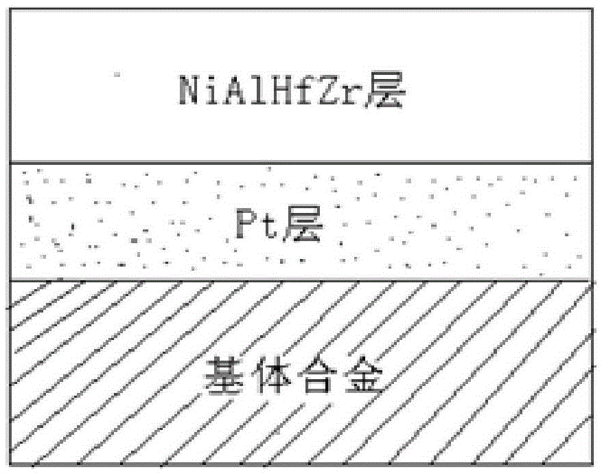
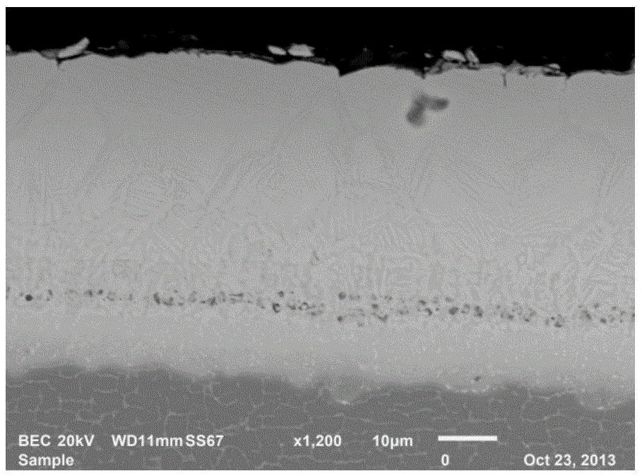
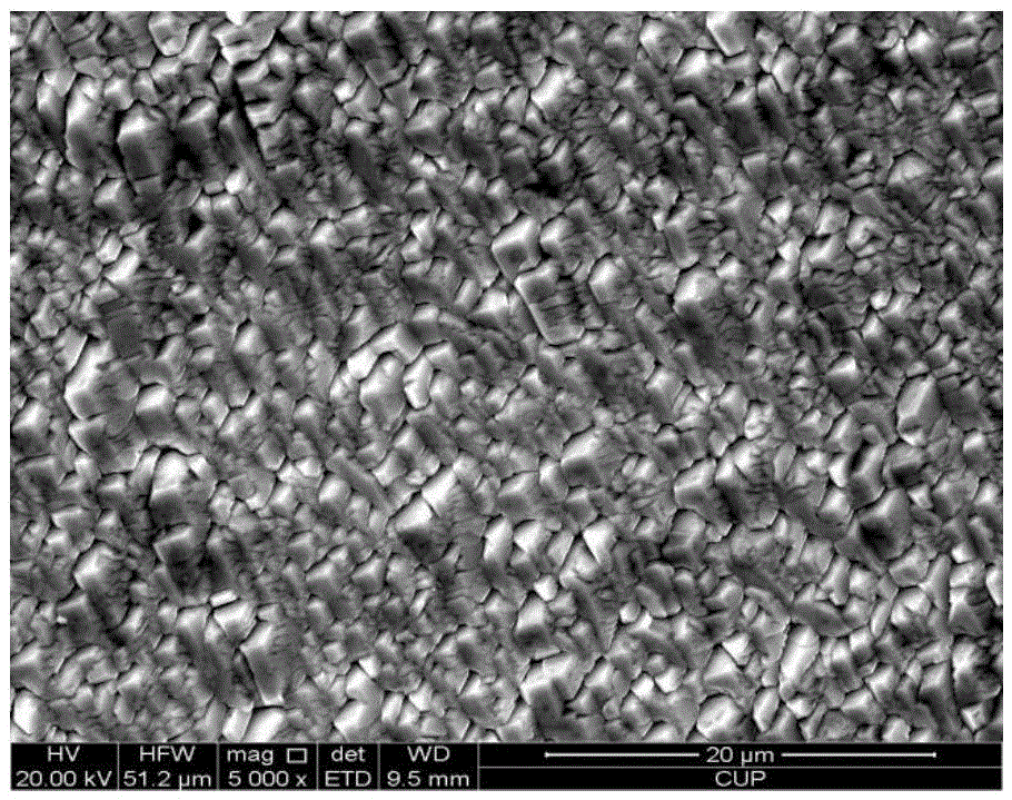
A 1200°C complete anti-oxidation binary trace active element-doped ptnial bonding layer and its preparation method
An active element and bonding layer technology, applied in the field of new thermal barrier coating bonding layer materials and their preparation, can solve problems such as affecting adhesion, improve bonding force, improve life, precisely control film thickness and uniformity sexual effect
- Summary
- Abstract
- Description
- Claims
- Application Information
AI Technical Summary
Problems solved by technology
Method used
Image
Examples
Embodiment 1
[0032] Example 1: A PtNiAl coating doped with binary trace active elements Hf and Zr was deposited on a N5 nickel-based single crystal superalloy substrate.
[0033] Step 1: Prepare the base material
[0034] The base material used is N5 nickel-based single crystal superalloy, and the base alloy is cut into specifications of 10×8×3mm by wire cutting. 3 Cut a hole with a diameter of 1mm at both ends of the sample, so that the sample can be hung on the bracket when preparing the coating. Then use 320#, 600#, and 800# water-grinding paper to grind all the six sides of the substrate in turn, so that the surface roughness of the substrate is Ra<0.8, fillet all 12 edges, and finally grind The good substrate samples were ultrasonically cleaned with absolute ethanol and acetone for 15 minutes in turn, dried and set aside.
[0035] Step 2: Electroplating or electron beam physical vapor deposition of Pt layer on the substrate
[0036] (A) If the Pt layer is prepared by electroplati...
Embodiment 2
[0049] Example 2 : Deposit binary trace active element Hf, Zr doped PtNiAl coating on IC211 nickel-based single crystal superalloy substrate.
[0050] Step 1: Prepare the base material
[0051] The matrix alloy used is IC211 nickel-based single crystal superalloy, and the matrix alloy is cut into specifications of 10×8×3mm by wire cutting. 3 Cut a hole with a diameter of 1mm at both ends of the sample, so that the sample can be hung on the bracket when preparing the coating. Then use 320#, 600#, and 800# water-grinding paper to grind all the six sides of the substrate in turn, so that the surface roughness of the substrate is Ra<0.8, fillet all 12 edges, and finally grind The good substrate samples were ultrasonically cleaned with absolute ethanol and acetone for 15 minutes in turn, dried and set aside.
[0052] Step 2: Electroplating or electron beam physical vapor deposition of Pt layer on the substrate
[0053] (A) If the Pt layer is prepared by electroplating:
[005...
Embodiment 3
[0066] Example 3: A PtNiAl coating doped with binary trace active elements Hf and Zr was deposited on a DD6 nickel-based single crystal superalloy substrate.
[0067] Step 1: Prepare the base material
[0068] The alloy matrix used is DD6 nickel-based single crystal superalloy, and the matrix alloy is cut into specifications of 10×8×3mm by wire cutting method 3 Cut a hole with a diameter of 1mm at both ends of the sample, so that the sample can be hung on the bracket when preparing the coating. Then use 320#, 600#, and 800# water-grinding paper to grind all the six sides of the substrate in turn, so that the surface roughness of the substrate is Ra<0.8, fillet all 12 edges, and finally grind The good substrate samples were ultrasonically cleaned with absolute ethanol and acetone for 15 minutes in turn, dried and set aside.
[0069] Step 2: Electroplating or electron beam physical vapor deposition of Pt layer on the substrate
[0070] (A) If the Pt layer is prepared by ele...
PUM
| Property | Measurement | Unit |
|---|---|---|
| diameter | aaaaa | aaaaa |
| thickness | aaaaa | aaaaa |
| thickness | aaaaa | aaaaa |
Abstract
Description
Claims
Application Information


