Method for manufacturing AlGaN-GaN heterojunction ohmic contact

A technology of ohmic contact and manufacturing method, which is applied in the field of microelectronics, can solve the problems of limited improvement of ohmic contact, achieve the possible effects of no stability problem, reduce ohmic contact resistance, and increase tunneling current

Inactive Publication Date: 2014-08-06
XIDIAN UNIV
View PDF4 Cites 18 Cited by
  • Summary
  • Abstract
  • Description
  • Claims
  • Application Information

AI Technical Summary

Problems solved by technology

However, this process has limited improvement on ohmic contact and usually needs to be used in conjunction with other methods

Method used


Image

  • Method for manufacturing AlGaN-GaN heterojunction ohmic contact
  • Method for manufacturing AlGaN-GaN heterojunction ohmic contact
  • Method for manufacturing AlGaN-GaN heterojunction ohmic contact

Examples


Embodiment 1

[0040] Embodiment 1: Fabricate an ohmic contact with a hole depth of 5nm and a metal Ti / Al / Ni / Au thickness of 20nm / 150nm / 40nm / 60nm.

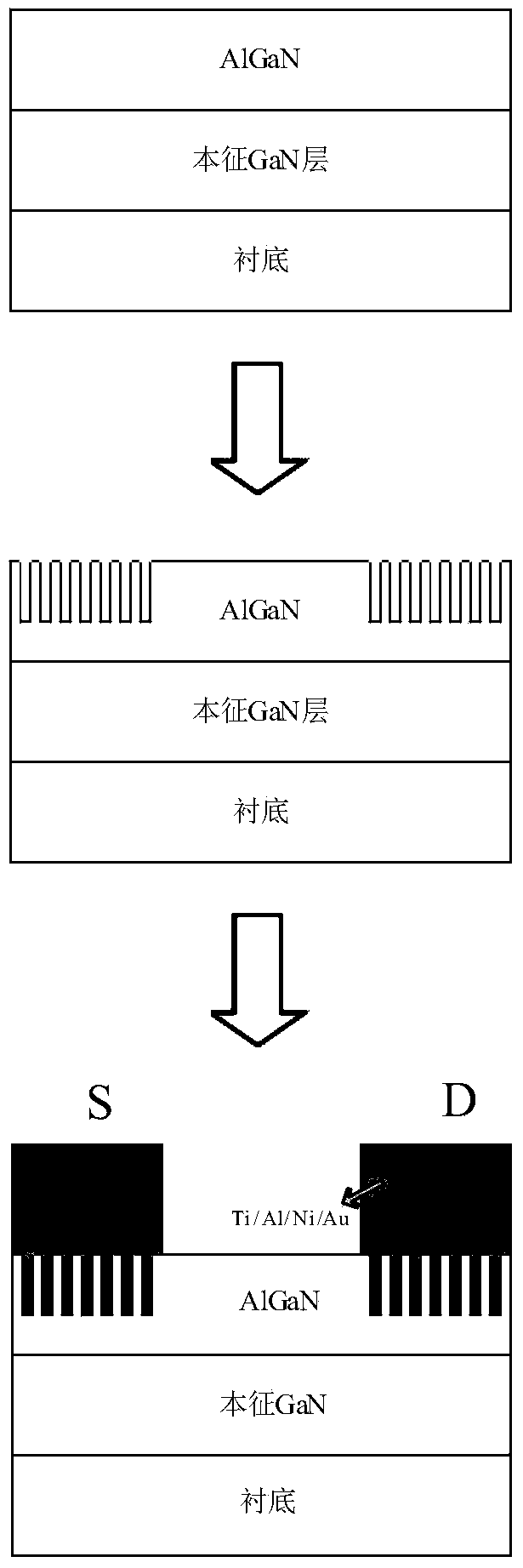
[0041] refer to figure 1 , the implementation steps of this example are as follows:

[0042] Step 1. Cleaning the AlGaN / GaN heterojunction material sample.

[0043] 1.1) Place the AlGaN / GaN heterojunction material sample in a 1:5 HF solution and soak for 30s to remove the surface oxide layer;

[0044] 1.2) The AlGaN / GaN heterojunction material sample was ultrasonically cleaned in acetone and ethanol organic solvents to remove surface contamination, and rinsed with deionized water for 5 minutes.

[0045] Step 2. Dig holes in the ohmic electrode area.

[0046] 2.1) Throw 0.6 μm positive glue EPI621 on the surface of the cleaned AlGaN / GaN heterojunction material sample at a speed of 5000 rpm with a glue throwing machine, and then put the glued AlGaN / GaN heterojunction material into the temperature Dry in a high-temperature oven at 110°C for 1mi...

Embodiment 2

[0056] Example 2: Fabricate an ohmic contact with a hole depth of 10 nm and a metal Ti / Al / Ni / Au thickness of 25 nm / 200 nm / 50 nm / 80 nm.

[0057] refer to figure 1 , the implementation steps of this example are as follows:

[0058] Step 1. Cleaning the AlGaN / GaN heterojunction material.

[0059] This step is the same as Step 1 in Example 1.

[0060] Step 2. Dig holes in the ohmic electrode area.

[0061] (2a) Spray 0.6 μm positive glue EPI621 on the surface of the cleaned AlGaN / GaN heterojunction material. The GaN heterojunction material is dried for 1 min, then exposed with an NSR1755I7A photolithography machine, and finally developed to obtain a photoresist mask with several through holes distributed in the ohmic electrode area. The sum of the areas of these through holes is the total area of ​​the ohmic contact electrodes 30% of;

[0062] (2b) Etch the AlGaN material exposed in the through hole of the photoresist mask with an RIE plasma dry etching machine, and the etchi...

Embodiment 3

[0071] Example 3: Fabricate an ohmic contact with a hole depth of 15 nm and a metal Ti / Al / Ni / Au thickness of 30 nm / 250 nm / 60 nm / 100 nm.

[0072] refer to figure 1 , the implementation steps of this example are as follows:

[0073] Step A. Cleaning the AlGaN / GaN heterojunction material.

[0074] This step is the same as Step 1 in Example 1.

[0075] Step B. Dig holes in the ohmic electrode area.

[0076](B1) Put the cleaned AlGaN / GaN heterojunction material into the glue-spinning machine, adjust the speed of the glue-spinning machine to 5000 rpm, and throw the positive glue EPI621 on the surface of the cleaned AlGaN / GaN heterojunction material. The AlGaN / GaN heterojunction material that has been glued is dried in a high-temperature oven at a temperature of 110°C for 1 min, then exposed with an NSR1755I7A photolithography machine, and finally developed to obtain an ohmic electrode area with several A photoresist mask for through holes, the sum of the areas of these through h...


PUM

PropertyMeasurementUnit
depthaaaaaaaaaa
thicknessaaaaaaaaaa
depthaaaaaaaaaa

Abstract

The invention discloses a method for manufacturing AlGaN-GaN heterojunction ohmic contact. The problems that in the prior art, contact resistance is large, the process is complex, and cost is high are mainly solved. The method comprises the manufacturing steps that (1), photoetching is carried out on the surface of AlGaN-GaN heterojunction, an etching mask with a plurality of through holes on an ohmic electrode region is obtained, and the sum of the areas of the exposed parts of the through holes is 15 percent to 45 percent of the area of an ohmic electrode; (2), etching hole digging with the depth of 5 nm to 15 nm is carried out on AlGaN materials exposed out of the through holes of the mask; (3), titanium / aluminum / nickel / gold multilayer metal is deposited on the AlGaN-GaN materials of a source region and a drain region with holes dug; (4), annealing of 800 DEG C to 870 DEG C is carried out on deposited electrode metal, and a source and drain ohmic contact electrode is formed. The method has the advantages that the process is simple and easy to control, and the ohmic contact resistance is low, and the method can be used for manufacturing AlGaN-GaN heterojunction high-frequency high-power high-electronic devices high in work efficiency and high in grain.

Description

technical field [0001] The invention belongs to the technical field of microelectronics, and relates to semiconductor materials and device manufacturing, in particular to a process manufacturing method for semiconductor device ohmic contacts, which can be used for manufacturing AlGaN / GaN heterojunction electronic devices. Background technique [0002] In recent years, the third bandgap semiconductor represented by SiC and GaN has the characteristics of large bandgap, high breakdown electric field, high thermal conductivity, high saturation electron velocity and high concentration of two-dimensional electron gas at the heterojunction interface, making it Widespread concern. In theory, high electron mobility transistor HEMT, light emitting diode LED, laser diode LD and other devices made of these materials have obvious superior characteristics than existing devices, so in recent years, researchers at home and abroad have conducted extensive and in-depth research on them. rese...

Claims


Application Information

Patent Timeline
Patent Type & Authority Applications(China)
IPC IPC(8): H01L21/28
CPCH01L29/41766H01L29/2003H01L29/7786H01L21/28575
Inventor 王冲钟仁骏陈冲何云龙郑雪峰马晓华郝跃
Owner XIDIAN UNIV
Why Eureka
Try Eureka