A diode selection element array structure and manufacturing method

A technology of an array structure and a manufacturing method, which is applied in the field of diode selection element array structure and manufacturing, can solve the problems of high deposition temperature, material quality, long time consumption, etc., and achieves the effect of simple process, low requirements and saving manufacturing cost.

Inactive Publication Date: 2016-10-05
陈秋峰
View PDF4 Cites 0 Cited by
  • Summary
  • Abstract
  • Description
  • Claims
  • Application Information

AI Technical Summary

Problems solved by technology

[0005] In the prior art, epitaxial silicon or selective epitaxial silicon is used as material to form PN junction diodes in phase change random access memory, and the manufacturing cost is expensive; in addition, due to the high deposition temperature of epitaxial silicon or selective epitaxial silicon, the requirements for the substrate surface are high, so that The process of manufacturing PN junction diodes is complex and takes a long time; at the same time, PN junction diodes are formed by stacking on the surface of the substrate, which has material quality problems

Method used


Image

  • A diode selection element array structure and manufacturing method
  • A diode selection element array structure and manufacturing method
  • A diode selection element array structure and manufacturing method

Examples


Embodiment Construction

[0040] The present invention will be described in detail below in conjunction with the accompanying drawings and specific embodiments.

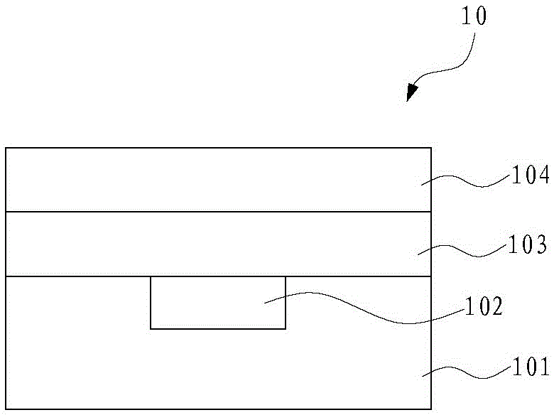
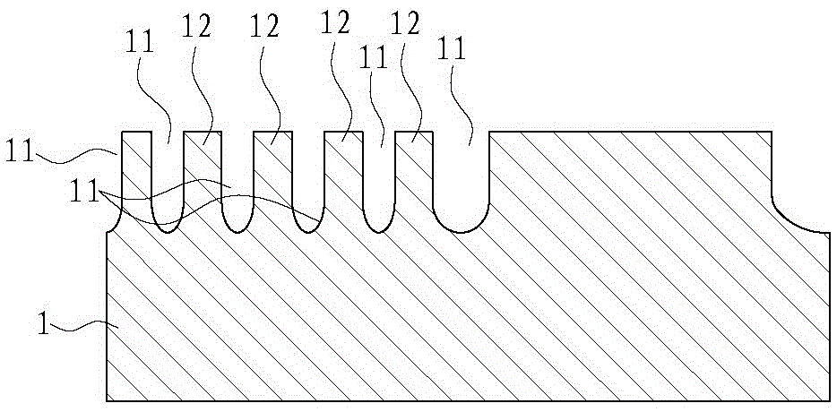
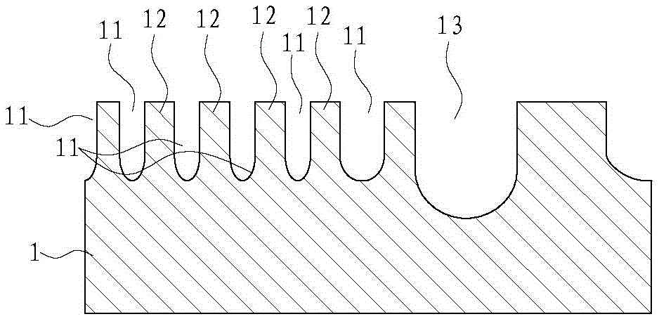
[0041] refer to Figure 2 to Figure 6 As shown, a method for manufacturing a diode selection element array structure disclosed in the present invention includes the following steps:

[0042] Such as figure 2 As shown, a P-type semiconductor substrate 1 is provided, and shallow isolation trenches 11 are formed at intervals on the P-type semiconductor substrate 1. The execution steps include forming a silicon oxide layer or a silicon nitride layer on the P-type semiconductor substrate 1, and performing optical The etching step includes opening the area of ​​the shallow isolation trench 11 by using an isolation mask, exposure, development, etc., and performing silicon etching by anisotropic dry etching to form the isolation trench 11 . The formation of the shallow isolation trenches 11 is a standard process, which will not be described in det...


PUM


Abstract

The invention discloses a diode selection element array structure manufacturing method. The diode selection element array structure manufacturing method includes forming shallow isolation grooves on a P-type semiconductor substrate at intervals, and forming blank posts among the shallow isolation grooves, wherein one of the blank posts is a P-tie blank post, and the rest are N-tie blank posts; filling the insulation layer in the shallow isolation grooves; forming an N trap on the P-type semiconductor substrate; burying a first P-type diffusion layer on the N trap; forming N-type diffusion layers on the N-tie blank posts, forming wolfram plugs on the N-type diffusion layers, and connecting the wolfram plugs with the N-type diffusion layers to form a first electrode of a diode; extending the P-tie blank posts to form second P-type diffusion layers, forming wolfram plugs on the second P-type diffusion layers, and connecting the wolfram plugs with the second P-type diffusion layers to form a second electrode of the diode; forming an N-type diffusion layer on the upper layer of one side of the N trap and forming another wolfram plug on the upper layer of the N-type diffusion layer and connecting the wolfram plug with the N-type diffusion layer to form a contact electrode of the N trap. The diode selection element array structure manufacturing method is simple in process, and manufacturing cost is saved; a diode selection element array structure formed by the manufacturing method is good in quality.

Description

technical field [0001] The invention relates to the technical field of semiconductors, in particular to a diode selection element array structure and a manufacturing method. Background technique [0002] Phase change random access memory has the characteristics of high read speed, low power, high capacity, high reliability, high write and erase times, low operating voltage / current and low cost. It is suitable for combining with CMOS technology and used as a higher density independent format or embedded memory applications. [0003] A phase change random access memory includes a storage node having a phase change layer, a transistor connected to the storage node, and a PN junction diode connected to the transistor. Depending on the voltage applied to it, the phase change layer changes from crystalline to amorphous, or vice versa. When the applied voltage is the set voltage, the phase change layer changes from an amorphous state to a crystalline state. When the applied volt...

Claims


Application Information

Patent Timeline
Patent Type & Authority Patents(China)
IPC IPC(8): H01L21/822H01L21/265H01L27/082
CPCH01L21/26506H01L21/8222H01L27/082
Inventor 陈秋峰王兴亚
Owner 陈秋峰
Why Eureka
Try Eureka