Method for preparing nano porous silicon by utilizing doped silicon particles

A nanoporous, silicon-doped technology, applied in nanotechnology, chemical instruments and methods, silicon compounds, etc., can solve the problems of restricting the application of porous silicon materials, the size of the base silicon material and the limited range of doping concentrations, etc. It has the effect of application value, good industrial value and strong operability

Active Publication Date: 2014-08-13
南京卓胜自动化设备有限公司
View PDF8 Cites 13 Cited by
  • Summary
  • Abstract
  • Description
  • Claims
  • Application Information

AI Technical Summary

Problems solved by technology

[0003] At present, the preparation of porous silicon is mainly obtained by using N-type or P-type silicon wafers or intrinsic bulk silicon particles as the matrix material through electrochemical etching, wet chemical etching and chemical etching. The size and doping concentration of the matrix silicon material The limited range of options, which limit the application of porous silicon materials
At present, it is still a challenge to obtain porous silicon or silicon nanowires by chemical etching using silicon particles with different doping concentrations. There are many bottlenecks, and industrial production has not yet been realized.

Method used


Image

  • Method for preparing nano porous silicon by utilizing doped silicon particles

Examples


Embodiment 1

[0029]This embodiment provides a method for preparing nanoporous silicon using doped silicon particles. When using doped silicon particles as a raw material, chemical etching is used to prepare nanoporous silicon. The specific steps are as follows:

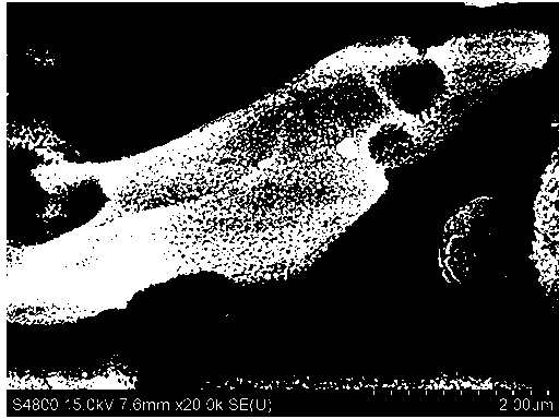
[0030] 1) The phosphorus doping concentration is selected to be 5.53×10 19 atoms / cm 3 (Conductivity 0.001~0.002Ω·cm) N-type single crystal silicon master alloy is used as raw material, processed by pulse discharge method, processing parameters are: open circuit voltage 150V; peak current 10A; pulse width 50μs; duty ratio 1:2, The working fluid is deionized water, and the electrodes are copper electrodes. Process and collect doped silicon particles, the particle size range of silicon particles is 1-10 μm, the size is concentrated at 5 μm, the concentration is greater than 90%, and the particles are block and spherical particles.

[0031] 2) Take 10g of silicon particles as the base material;

[0032] 3) Cleaning the surface of t...

Embodiment 2

[0041] This embodiment provides a method for preparing nanoporous silicon using doped silicon particles. When using doped silicon particles as a raw material, chemical etching is used to prepare nanoporous silicon. The specific steps are as follows:

[0042] 1) The boron doping concentration is selected to be 5×10 18 atoms / cm 3 (Conductivity 0.01~0.02Ω·cm) P-type polysilicon ingot is used as raw material, processed by pulse discharge method, the processing parameters are: open circuit voltage 100V; peak current 5A; pulse width 20μs; duty ratio 1:5, working fluid is Deionized water, the electrode is a copper electrode. Process and collect doped silicon particles, the particle size range of silicon particles is 1-5 μm, the size is concentrated at 2 μm, the concentration is greater than 90%, and the particles are spherical particles.

[0043] 2) Take 10g of silicon particles as the base material;

[0044] 3) Cleaning the surface of the silicon particles with a chemical solutio...


PUM

PropertyMeasurementUnit
sizeaaaaaaaaaa
particle diameteraaaaaaaaaa
sizeaaaaaaaaaa

Abstract

The invention discloses a method for preparing nano porous silicon by utilizing doped silicon particles. The method comprises the following steps: selecting silicon particles with a certain doping concentration, washing with hydrofluoric acid, then enabling the silicon particles to react in a solution which is prepared by selecting nitrate, hydrofluoric acid and oxidant with assistance of ultrasonic process centrifugally washing the silicon particles, and finally washing the silicon particles by using dilute nitric acid to obtain the three-dimensional nano porous silicon. The optimal process parameters such as best constitution of chemical etching corrosive agent, volume ratio and specific concentration of a reaction reagent, reaction time, reaction temperature, ultrasonic frequency, processing time and the like are screened out through a great number of experiments, and the prepared high-purity three-dimensional doped porous silicon is regular in pore shape, uniform in distribution and applicable to the fields such as lithium batteries, solar batteries, semiconductors and sensors. The method is strong in process maneuverability, low in cost, high in yield and applicable to industrialized mass production.

Description

technical field [0001] The invention relates to the field of preparation of porous silicon materials, in particular to a method for preparing sponge-like nanoporous silicon with controllable structure by using doped silicon particles by electrochemical etching. Background technique [0002] Porous silicon material has unique optoelectronic properties and large specific surface area so that it can be used in various detectors, biological microsensors, optoelectronic nano-devices, energy storage materials and other fields, especially as the anode material of lithium batteries has attracted much attention in recent years. Compared with traditional negative electrode materials, silicon has an ultra-high theoretical specific capacity (4200mAh / g) and a low delithiation potential (<0.5V), and it is difficult to cause lithium precipitation on the surface during charging, and its safety performance is better. At present, silicon has become a One of the potential options for upgrad...

Claims


Application Information

Patent Timeline
Patent Type & Authority Applications(China)
IPC IPC(8): H01M4/38B82Y40/00
CPCB82Y40/00C01B33/021H01M4/386H01M10/0525Y02E60/10
Inventor 洪捐
Owner 南京卓胜自动化设备有限公司
Why Eureka
Try Eureka