Multi-layer flexible circuit board and process for producing the same

A flexible printed circuit, flexible printing technology, applied in the direction of multilayer circuit manufacturing, printed circuit manufacturing, printed circuit, etc., can solve the problems of poor yield, excessive cost, difficult plating, etc., to improve the quality Rate problem, reduce material waste, reduce the effect of thickness

Active Publication Date: 2014-08-13
ICHIA TECH
View PDF3 Cites 7 Cited by
  • Summary
  • Abstract
  • Description
  • Claims
  • Application Information

AI Technical Summary

Problems solved by technology

[0002] Known flexible printed circuit boards are all obtained by processing and manufacturing a semi-finished product of a precursor substrate. The precursor substrate needs to be coated with a metal conductive layer to facilitate subsequent processing and manufacturing. Generally speaking, the material of these substrates is The surface is inherently difficult to be attached to the metal. For this reason, the known treatment methods include metal spraying method, sputtering method, CVD, evaporation method, and dry plating method, etc. However, these methods will cause the precursor substrate The thickness of the semi-finished product is thick or the plating is difficult or the plating time is too long
Excessive thickness will not be conducive to the current trend of product miniaturization
[0003] Moreover, the problem of thicker thickness is not conducive to the manufacture of multi-layer flexible printed circuit boards; the problem of difficult plating and long plating time will lead to limited production capacity and excessive cost.
In addition, multi-layer flexible printed circuit boards are mostly produced by lamination. This known method often has lamination defects, and then bubbles are generated due to structural gaps, resulting in poor yields. good
[0004] In addition, there are many multi-layer electrical circuits, and the problem of crosstalk between electrical circuits is serious, which is also a problem to be solved.

Method used


Image

  • Multi-layer flexible circuit board and process for producing the same
  • Multi-layer flexible circuit board and process for producing the same
  • Multi-layer flexible circuit board and process for producing the same

Examples


no. 1 example

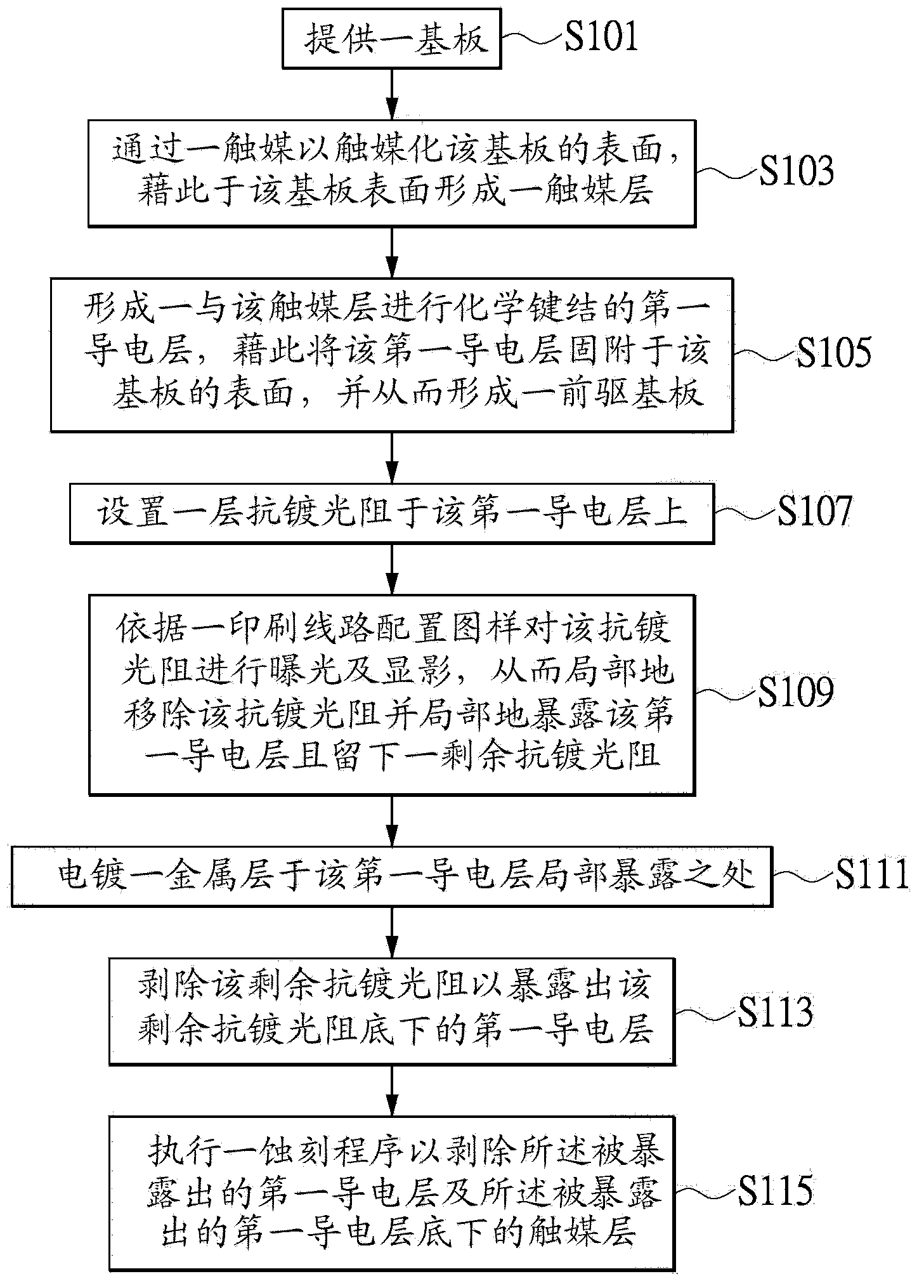
[0036] see Figure 1A As shown, it is a flow chart of the steps of the first embodiment of the present invention. The present invention provides a method for manufacturing a flexible printed circuit board, which includes the following steps:

[0037] please cooperate Figure 2A As shown in the evolution diagram of the cross-sectional structure, a substrate 10 is provided. The substrate 10 has a surface 11. The surface 11 of the substrate 10 also includes an upper surface 11a and a lower surface 11b. The substrate 10 is a raw material, and its material can be poly Imide (Polyimide, PI), polyester (Polyethylene Terephthalate Polyester, PET), polyethylene glycol dicarboxylate (Polyethylene Naphthalate, PEN), polytetrafluoroethylene (Polytetrafluoroethylene, PTFE), liquid crystal polymer (Thermotropic Liquid Crystal Polymer) , LCP), epoxy resin (Epoxy), aramid (Aramid) and other high molecular polymers. cooperate again Figure 2B As shown, then laser processing can be used accor...

no. 2 example

[0057] In another embodiment, such as image 3 is shown in the flow chart of the steps and please also refer to Figure 4A , Figure 4B and Figure 4C As shown in the evolution schematic diagram of the cross-sectional structure of the present invention, the present invention also provides a kind of manufacturing method of the multi-layer flexible printed circuit board, comprising: providing a flexible printed circuit board P, its surface 11 also includes upper surface 11a and The lower surface 11b, and the surface 11 includes a first electrical circuit unit E1 protruding relative to the surface 11 and a vacant portion 11c where the first electrical circuit unit E1 is not laid (step S301 ). An electrical insulating layer is laid on the surface 11 of the flexible printed circuit board P, so that the electrical insulating layer fills the above-mentioned vacancy 11c to define an adjacent spacer layer 10a, and the electrical insulating layer covers the first electrical The top o...

no. 3 example

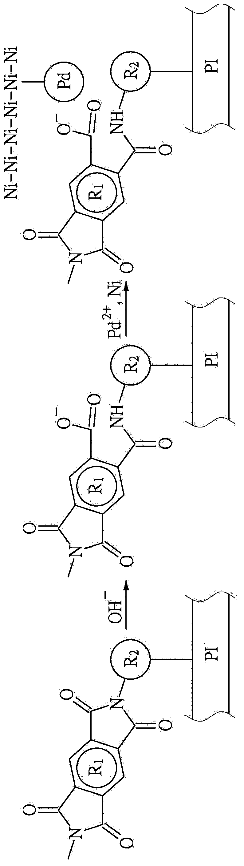
[0072] yes come back Figure 2A , Figure 2B and Figure 2C As shown, the present invention also provides a precursor substrate (number omitted) as a semi-finished printed circuit board, and used as a subsequent processing and manufacturing of the finished printed circuit board, which at least includes: a substrate 10 and a first conductive layer 30. The substrate 10 has a surface 11 , which is a catalyzed surface, and the catalyzed surface further includes a catalyst layer 20 . The first conductive layer 30 is combined with the catalyst layer 20 , so that the first conductive layer 30 can cover the surface 11 of the substrate 11 .

[0073] Preferably, the material of the substrate 10 is polyimide; and the catalyst layer 20 also includes a palladium catalyst; , Electroless plating of any of the cobalt alloys.

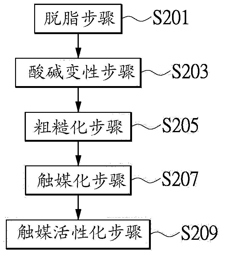
[0074] Preferably, the above-mentioned surface 11 further includes at least an upper surface 11a and a lower surface 11b , and the substrate 10 further defines a v...


PUM


Abstract

The present invention provides a multi-layer flexible circuit board, comprising at least an electric circuit disposed on a vertical interval layer, wherein at least two sides of the electric circuit are covered by neighboring interval layer and another vertical interval composed layer of electric insulating material. The disclosure provides a non-pressing way to stack the multi-layer flexible circuit board, thereby preventing disjunctions between layers, reducing the product thickness, increasing yield rate, and reducing crosstalk between electric circuits.

Description

technical field [0001] The invention relates to a multi-layer flexible printed circuit board and its manufacturing method, in particular to a multi-layer flexible printed circuit board stacked mainly by covering at least two sides of the electrical circuit unit with an electrical insulating layer. Flexible printed circuit board and its manufacturing method. Background technique [0002] Known flexible printed circuit boards are all obtained by processing and manufacturing a semi-finished product of a precursor substrate. The precursor substrate needs to be coated with a metal conductive layer to facilitate subsequent processing and manufacturing. Generally speaking, the material of these substrates is The surface is inherently difficult to be attached to the metal. For this reason, the known treatment methods include metal spraying method, sputtering method, CVD, evaporation method, and dry plating method, etc. However, these methods will cause the precursor substrate The t...

Claims


Application Information

Patent Timeline
Patent Type & Authority Applications(China)
IPC IPC(8): H05K1/02H05K3/46
CPCH05K3/4673H05K3/426H05K1/0393H05K3/0011H05K3/4644H05K1/0216H05K3/108H05K1/02H05K3/46
Inventor 丘建华赵治民郭培荣江嘉华萧智诚管丰平李英玮庄永昌
Owner ICHIA TECH
Why Eureka
Try Eureka