Crystalline silicon battery surface passive film and manufacturing method thereof

A technology of crystalline silicon battery and passivation film, which is applied in the manufacture of circuits, electrical components, and final products. It can solve the problems of escaping silicon wafers and insignificant differences in refractive index, and achieve good light transmission and anti-PID effects. , The effect of improving battery efficiency

Inactive Publication Date: 2014-08-20
ALTUSVIA ENERGY TAICANG
View PDF3 Cites 14 Cited by
  • Summary
  • Abstract
  • Description
  • Claims
  • Application Information

AI Technical Summary

Problems solved by technology

In addition, the silicon nitride film is a gradient film, the difference in refractive index between the film layers is not obvious, the probability of total reflection is small, and a large part will escape from the silicon wafer.

Method used


Image

  • Crystalline silicon battery surface passive film and manufacturing method thereof
  • Crystalline silicon battery surface passive film and manufacturing method thereof

Examples


Embodiment 1

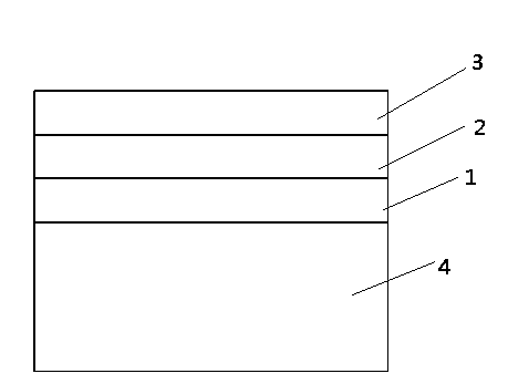
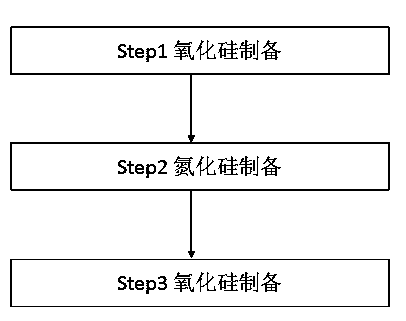
[0027] The production method is as follows: the N-type surface 4 of the P-type crystalline silicon battery is sequentially subjected to the following conventional procedures: primary cleaning, diffusion and secondary cleaning, and the first layer of silicon oxide film is produced by PECVD. The process conditions are: temperature 360 ​​° C, The nitrogen flow rate is 20L / min, the laughing gas flow rate is 7L / min, the silane flow rate is 2.1L / min, the pressure is 1Torr, the radio frequency power is 5kW, and the duration is 12s to obtain the first silicon oxide film 1 with a thickness of 20nm and a refractive index of 1.5; then use The second layer of silicon nitride film 2 is produced on the first silicon oxide film 1 by PECVD method. The process conditions are: temperature 360°C, nitrogen flow rate 25L / min, ammonia flow rate 0.6L / min, silane flow rate 1.9L / min, pressure 1.2Torr, RF power 8kW, duration 35s, to obtain a silicon nitride film 2 with a thickness of 45nm and a refracti...


PUM

PropertyMeasurementUnit
thicknessaaaaaaaaaa
thicknessaaaaaaaaaa
thicknessaaaaaaaaaa

Abstract

The invention discloses a crystalline silicon battery surface passive film and a manufacturing method of the crystalline silicon battery surface passive film. The crystalline silicon battery surface passive film comprises a first silicon oxide film, a silicon nitride film and a second silicon oxide film. The silicon nitride film is deposited on the first silicon oxide film. The second silicon oxide film is deposited on the silicon oxide film. The thickness d1 of the first silicon oxide film is 10 nm-30 nm. The thickness d2 of the silicon nitride film is 30 nm-50 nm. The thickness d3 of the second silicon oxide film is 25 nm-50 nm. The probability of light full reflection is substantially increased, and namely more light enters a silicon wafer, so that more charge carriers are generated, and battery efficiency is improved.

Description

technical field [0001] The invention relates to a passivation film on the surface of a crystalline silicon battery and a preparation method thereof. Background technique [0002] Potential-Induced Degradation (PID, Potential-Induced Degradation) is ubiquitous in traditional photovoltaic modules. According to the results of many domestic and foreign research institutions, the main reason for PID is: as the number of photovoltaic modules in series continues to increase, photovoltaic The probability that components will withstand high voltage-to-ground potential energy is also increasing. When one end of the system is grounded, the component farthest from the ground will generate a higher ground potential, which is close to 1000v in European design standards. Under such a high voltage, leakage current will be generated and power generation will be lost. The leakage current generally flows into the ground through the aluminum frame, packaging material and mounting bracket, and ...

Claims


Application Information

Patent Timeline
Patent Type & Authority Applications(China)
IPC IPC(8): H01L31/0216H01L31/18
CPCH01L31/02167Y02P70/50
Inventor 张辉杨红冬刘仁中张斌邢国强
Owner ALTUSVIA ENERGY TAICANG
Why Eureka
Try Eureka