LED epitaxial wafer growing on metal Al substrate and preparing method and application thereof

A technology for LED epitaxial wafers and substrates, which is used in semiconductor/solid-state device manufacturing, electrical components, circuits, etc., can solve the problems of unstable chemical properties of metal Al substrates, difficulty in thin film epitaxy, and affecting the quality of epitaxial thin film growth, etc. Achieve the effect of improving internal quantum efficiency, shortening nucleation time, and excellent thermal conductivity

Active Publication Date: 2014-08-20
广州市众拓光电科技有限公司
View PDF4 Cites 5 Cited by
  • Summary
  • Abstract
  • Description
  • Claims
  • Application Information

AI Technical Summary

Problems solved by technology

[0006] However, the metal Al substrate is chemically unstable. When the epitaxial temperature is higher than 700 °C, the interface reaction between the epitaxial nitride and the metal substrate will seriously affect the quality of the epitax

Method used


Image

  • LED epitaxial wafer growing on metal Al substrate and preparing method and application thereof
  • LED epitaxial wafer growing on metal Al substrate and preparing method and application thereof
  • LED epitaxial wafer growing on metal Al substrate and preparing method and application thereof

Examples


Example Embodiment

[0050] Example 1

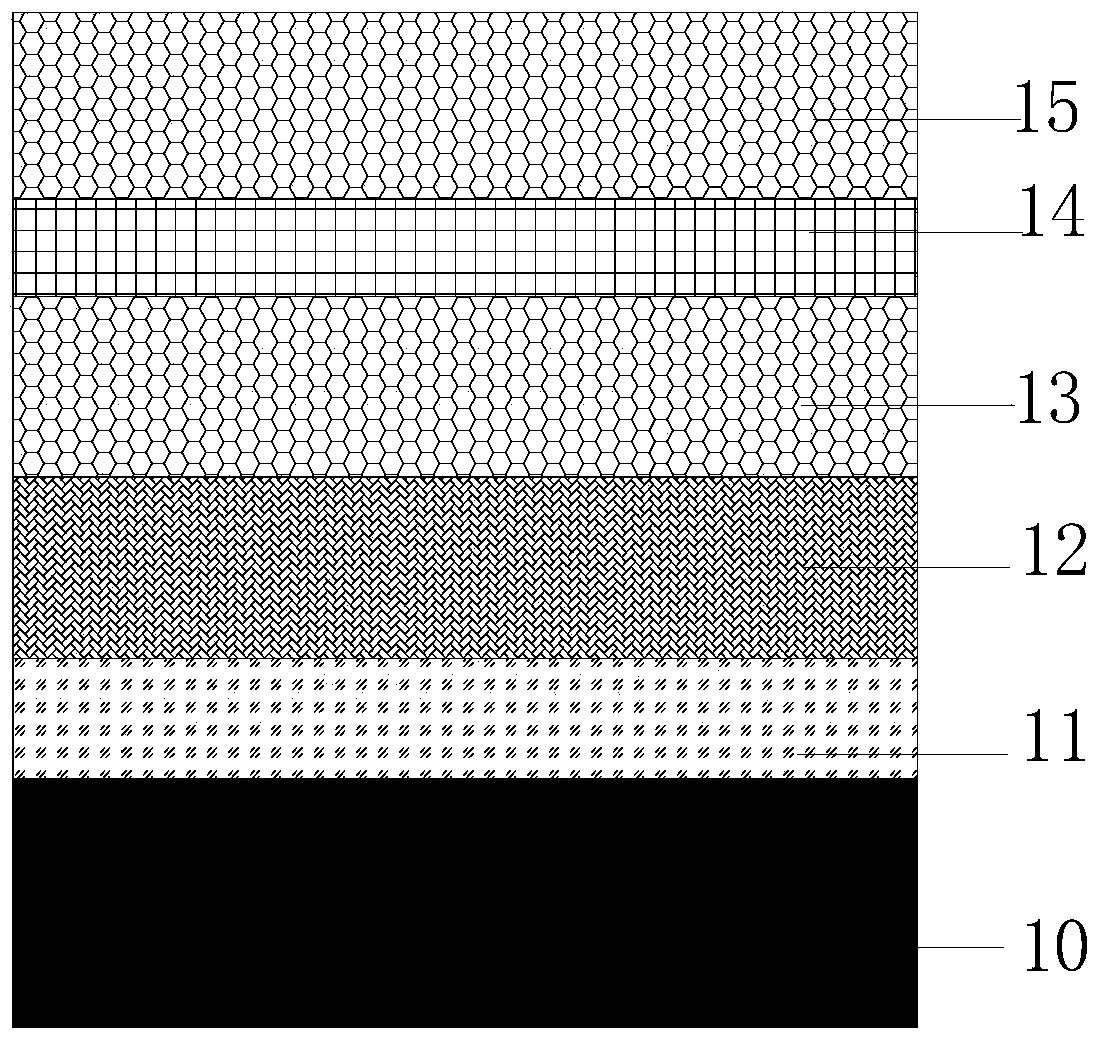
[0051] An LED epitaxial wafer grown on a metal Al substrate, which is prepared by the following method:

[0052] 1) Substrate treatment: select metal Al as the substrate, and polish the surface of the Al substrate with diamond slurry. Use a microscope to observe the surface of the substrate when there are no scratches, then use chemical mechanical polishing to polish the substrate. The bottom is polished; then the cleaned substrate is placed in deionized water for ultrasonic cleaning at room temperature for 5 minutes to remove the dirt particles on the surface of the Al substrate, and then washed with hydrochloric acid, acetone, and ethanol to remove organic matter on the surface; after cleaning The substrate is dried with dry nitrogen with a purity of 99.9999%; finally the substrate Al is placed at a pressure of 2×10 -10 In the growth chamber of Torr's UHV-PLD, bake at 450°C for 1 hour to remove contaminants on the substrate surface, and then air-cool to room te...

Example Embodiment

[0066] Example 2

[0067] An LED epitaxial wafer grown on a metal Al substrate, which is prepared by the following method:

[0068] 1) Substrate treatment: select metal Al as the substrate, and polish the surface of the Al substrate with diamond slurry. Use a microscope to observe the surface of the substrate when there are no scratches, then use chemical mechanical polishing to polish the substrate. The bottom is polished; then the cleaned substrate is placed in deionized water for ultrasonic cleaning at room temperature for 5 minutes to remove the dirt particles on the surface of the Al substrate, and then washed with hydrochloric acid, acetone, and ethanol to remove organic matter on the surface; after cleaning The substrate is dried with dry nitrogen with a purity of 99.9999% (v%); finally, the substrate Al is placed at a pressure of 2×10 -10 In the growth chamber of Torr's UHV-PLD, bake at a high temperature of 500°C for 1 hour to remove contaminants on the substrate surface, ...

Example Embodiment

[0082] Example 3

[0083] An LED epitaxial wafer grown on a metal Al substrate, which is prepared by the following method:

[0084] 1) Substrate treatment: select metal Al as the substrate, and polish the surface of the Al substrate with diamond slurry. Use a microscope to observe the surface of the substrate when there are no scratches, then use chemical mechanical polishing to polish the substrate. The bottom is polished; then the cleaned substrate is placed in deionized water for ultrasonic cleaning at room temperature for 5 minutes to remove the dirt particles on the surface of the Al substrate, and then washed with hydrochloric acid, acetone, and ethanol to remove organic matter on the surface; after cleaning The substrate is dried with dry nitrogen with a purity of 99.9999%; finally the substrate Al is placed at a pressure of 2×10 -10 In the growth chamber of Torr's UHV-PLD, bake at a high temperature of 550°C for 1 hour to remove contaminants on the substrate surface, and th...


PUM

PropertyMeasurementUnit
Thicknessaaaaaaaaaa
Thicknessaaaaaaaaaa
Thicknessaaaaaaaaaa

Abstract

The invention discloses an LED epitaxial wafer growing on a metal Al substrate. The LED epitaxial wafer comprises the metal Al substrate, an Al2O3 protecting layer growing on the metal Al substrate with a metal Al substrate crystal face (111) as an epitaxial face, a U-GaN thin film layer, an N-GaN thin film layer, an InGaN/GaN multi-quantum-well layer and a p-type GaN thin film. The epitaxy orientation relationship of the U-GaN thin film layer, the N-GaN thin film layer, the InGaN/GaN multi-quantum-well layer and the p-type GaN thin film is GaN (0001)//Al2O3 (0001)//Al (111), and the U-GaN thin film layer, the N-GaN thin film layer, the InGaN/GaN multi-quantum-well layer and the p-type GaN thin film grow on the Al2O3 protecting layer from bottom to top. By selecting proper crystal orientation, a high-quality GaN epitaxial thin film is obtained on the Al (111) substrate, and accordingly the light emitting efficiency of an LED is improved.

Description

technical field [0001] The present invention relates to the technical field of film synthesis by metal-organic chemical vapor deposition, in particular to an LED epitaxial wafer grown on a metal Al substrate and its preparation method and application; it is mainly used in bulk acoustic wave resonators with various dielectric layers , logic circuits, light emitting diodes, photoelectric thin film devices, solar cells, photodiodes, photodetectors, lasers and other fields. Background technique [0002] Light-emitting diode (LED), as a new type of solid-state lighting source and green light source, has outstanding features such as small size, low power consumption, environmental protection, long service life, high brightness, low heat and colorful, and is widely used in outdoor lighting, commercial lighting and decoration Engineering and other fields have a wide range of applications. At present, under the background of the increasingly serious problem of global warming, saving...

Claims


Application Information

Patent Timeline
IPC IPC(8): H01L33/02H01L33/12H01L33/00
CPCH01L33/16H01L21/02425H01L21/02488H01L21/0254H01L21/02631H01L33/0066H01L33/0075H01L33/12
Inventor 李国强
Owner 广州市众拓光电科技有限公司
Why Eureka
Try Eureka