LED epitaxial wafer growing on Ag substrate and preparing method and application of LED epitaxial wafer

A technology of LED epitaxial wafers and substrates, applied in semiconductor/solid-state device manufacturing, electrical components, circuits, etc., can solve problems such as difficulties in film epitaxy, affecting the quality of epitaxial film growth, and unstable chemical properties of metal Ag substrates. Achieve the effect of improving internal quantum efficiency, avoiding high temperature interface reaction, and uniform current distribution

Active Publication Date: 2014-08-20
广州市众拓光电科技有限公司
View PDF4 Cites 8 Cited by
  • Summary
  • Abstract
  • Description
  • Claims
  • Application Information

AI Technical Summary

Problems solved by technology

[0006] However, the metal Ag substrate is chemically unstable. When the epitaxial temperature is higher than 620°C, the interface reaction between the epitaxial nitride and the metal substrate will seriously affect the quality of the epitax

Method used


Image

  • LED epitaxial wafer growing on Ag substrate and preparing method and application of LED epitaxial wafer
  • LED epitaxial wafer growing on Ag substrate and preparing method and application of LED epitaxial wafer
  • LED epitaxial wafer growing on Ag substrate and preparing method and application of LED epitaxial wafer

Examples


Embodiment 1

[0044] A method for preparing an LED epitaxial wafer grown on an Ag substrate, comprising the following steps:

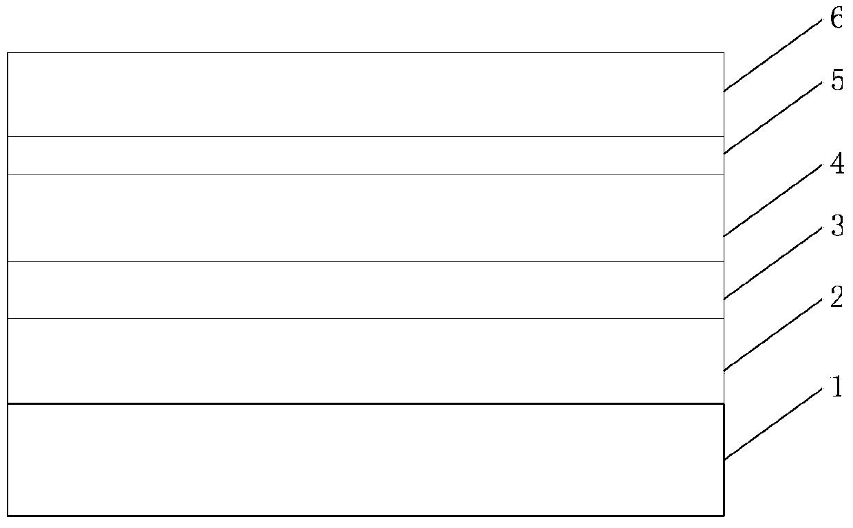
[0045] 1) Selection of the substrate and its crystal orientation: Ag substrate is used, the (111) plane is used as the epitaxial plane, and the crystal epitaxial orientation relationship is: AlN[11-20] / / Ag[1-10];

[0046] 2) Polishing, cleaning and annealing of the substrate surface: first, the surface of the Ag substrate is polished with diamond slurry, and the surface of the substrate is observed with an optical microscope until there are no scratches, and then the chemical mechanical polishing method is used for polishing; Secondly, the Ag substrate was ultrasonically cleaned in deionized water at room temperature for 5 minutes to remove the sticky particles on the surface of the Ag substrate, then washed with acetone and ethanol in order to remove the surface organic matter, and dried with high-purity dry nitrogen; finally, the Ag substrate was The substrate is ...

Embodiment 2

[0060] A method for preparing an LED epitaxial wafer grown on an Ag substrate, comprising the following steps:

[0061] 1) Selection of the substrate and its crystal orientation: Ag substrate is used, the (111) plane is used as the epitaxial plane, and the crystal epitaxial orientation relationship is: AlN[11-20] / / Ag[1-10];

[0062] 2) Polishing, cleaning and annealing of the substrate surface: first, the surface of the Ag substrate is polished with diamond slurry, and the surface of the substrate is observed with an optical microscope until there are no scratches, and then the chemical mechanical polishing method is used for polishing; Secondly, the Ag substrate was ultrasonically cleaned in deionized water at room temperature for 4 minutes to remove the sticky particles on the surface of the Ag substrate, then washed with acetone and ethanol in sequence to remove surface organic matter, and dried with high-purity dry nitrogen; finally, the Ag substrate was The substrate is p...


PUM

PropertyMeasurementUnit
Thicknessaaaaaaaaaa
Thicknessaaaaaaaaaa
Thicknessaaaaaaaaaa

Abstract

The invention discloses an LED epitaxial wafer growing on an Ag substrate. The LED epitaxial wafer growing on the Ag substrate comprises the Ag substrate, an AlN buffer layer, a U-GaN film layer, an N-GaN film layer, an InGaN/GaN multi-quantum-well layer and a P-GaN film. The AlN buffer layer, the U-GaN film layer, the N-GaN film layer, the InGaN/GaN multi-quantum-well layer and the P-GaN film sequentially grow on the Ag substrate. By the adoption of the low-temperature growth technology, a GaN film grows on the novel metal Ag substrate in an epitaxial mode, so that the LED epitaxial wafer with the high quality is obtained; by the adoption of the metal Ag substrate, the growth technology is simple, the price is low, and the manufacturing cost of a device can be reduced to a great extent; by the selection of the proper crystal orientation, the GaN epitaxial film with the high quality is obtained from the Ag substrate (111) and the efficiency of nitride devices such as a photoelectric detector can be improved to a great extent.

Description

technical field [0001] The invention relates to an LED epitaxial wafer, in particular to an LED epitaxial wafer grown on an Ag substrate, a preparation method and application thereof. Background technique [0002] Light-emitting diode (LED), as a new type of solid-state lighting source and green light source, has outstanding features such as small size, low power consumption, environmental protection, long service life, high brightness, low heat and colorful, and is widely used in outdoor lighting, commercial lighting and decoration Engineering and other fields have a wide range of applications. At present, under the background of the increasingly serious problem of global warming, saving energy and reducing greenhouse gas emissions has become an important issue faced by the whole world. A low-carbon economy based on low energy consumption, low pollution, and low emissions will become an important direction of economic development. In the field of lighting, the application...

Claims


Application Information

Patent Timeline
IPC IPC(8): H01L33/02H01L33/00
CPCH01L21/02425H01L21/02458H01L21/0254H01L21/0262H01L21/02631H01L33/0066H01L33/0075H01L33/12
Inventor 李国强
Owner 广州市众拓光电科技有限公司
Why Eureka
Try Eureka