Crucible for preparing polycrystalline silicon ingot and growth method of polycrystalline silicon ingot

A technology for polycrystalline silicon ingots and crucibles, which is applied in the directions of polycrystalline material growth, single crystal growth, crystal growth, etc. It can solve the problems of poor repeating effect, increased cost of casting ingots, and complicated crucible structure, so as to increase the size and improve the utilization rate , Improve the effect of electrical performance

Active Publication Date: 2014-09-03
郎溪品旭科技发展有限公司
View PDF6 Cites 1 Cited by
  • Summary
  • Abstract
  • Description
  • Claims
  • Application Information

AI Technical Summary

Problems solved by technology

Chinese patent application 201010198142.5 discloses a method for growing quasi-single crystal silicon using seed crystals. Although the method reuses the seed crystals, it uses the silicon ingot head and tail as the next growth seed crystal. Due to the silicon ingot head and tail It contains a lot of impurities and defects, and the repeat effect is not good
Chinese patent application 201010564154.5 discloses a crucible and a method for growing quasi-single crystal silicon using the crucible. The structure of this type of crucible is complex, and if the seed crystal is used, the cost of ingot casting will not only be increased, but the difficulty will also increase a lot.

Method used


Image

  • Crucible for preparing polycrystalline silicon ingot and growth method of polycrystalline silicon ingot
  • Crucible for preparing polycrystalline silicon ingot and growth method of polycrystalline silicon ingot
  • Crucible for preparing polycrystalline silicon ingot and growth method of polycrystalline silicon ingot

Examples


Embodiment 1

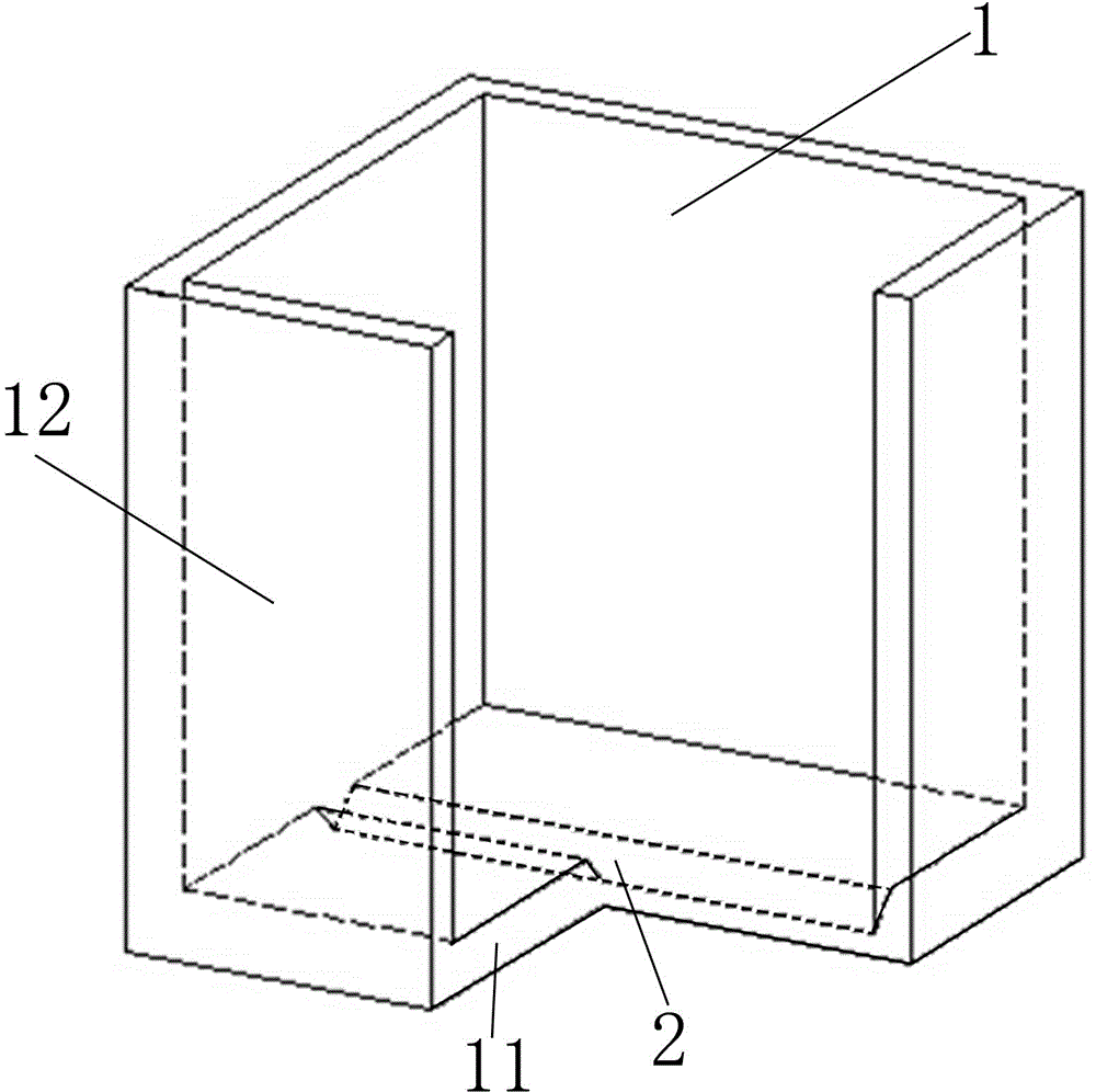
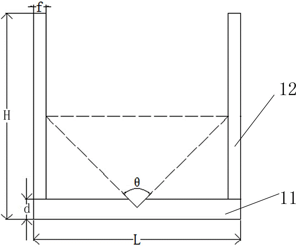
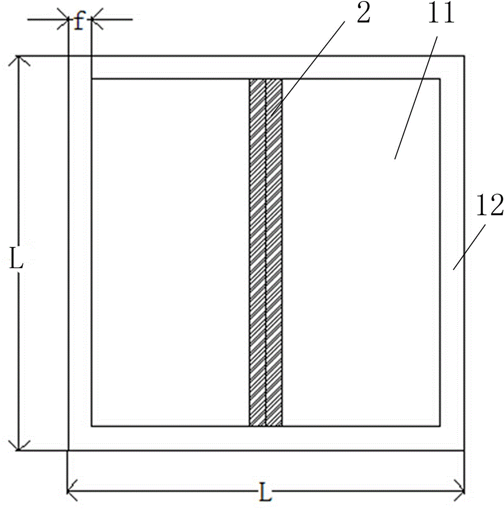
[0030] There is a crucible 1 with a "V"-shaped long groove 2 on the bottom surface, and the cross-sectional view of its structure is as follows figure 2 As shown, the thickness f of the crucible wall 12 is 12 mm, the thickness d of the bottom surface 11 is 20 mm, the side length L of the bottom surface 11 is 198 mm, and the height H of the crucible wall 12 is 200 mm; The center line of the bottom surface 11 is parallel to one side of the square bottom surface 11; the depth h of the "V"-shaped long groove 2 is 8 mm, and the angle θ between the two hypotenuses of the "V"-shaped long groove is 90 degrees. The inner wall of crucible 1 is sprayed with silicon nitride, and heat-treated at 1050 °C for 5 hours to form a dense silicon nitride coating; 6 kg of P-type polysilicon raw material with a purity of 6N is placed in crucible 1 according to a certain method; The furnace body is evacuated to a vacuum of 10 Pa and starts to heat; use argon as a protective gas; heat to 1540 °C unde...

Embodiment 2

[0033] A crucible 1 with two "V"-shaped long grooves 2 is opened on the bottom surface, and the cross-sectional view of its structure is as follows Figure 5 As shown, the thickness f of the crucible wall 12 is 12 mm, the thickness d of the bottom surface 11 is 20 mm, the side length L of the bottom surface 11 is 198 mm, and the height H of the crucible wall 12 is 200 mm. The center of the bottom surface 11 is parallel to the line of symmetry on one side and is distributed symmetrically. The intersection of the extension lines on both sides of the two "V"-shaped long grooves 2 and the crucible wall 12 and the extension line of the adjacent sides of the two "V"-shaped long grooves 2 The intersection points are at the same height, the vertical distance h2 from the intersection point to the inner bottom of the crucible is 36 mm, the depth h of the "V"-shaped long groove 2 is 8 mm, and the angle θ between the two hypotenuses of the "V"-shaped long groove 2 is 90 degrees. The proce...

Embodiment 3

[0035] A crucible 1 with three "V"-shaped long grooves 2 is opened on the bottom surface, and the cross-sectional view of its structure is as follows Figure 6 As shown, the thickness f of the crucible wall 12 is 12 mm, the thickness d of the bottom surface 11 is 20 mm, the side length L of the bottom surface 11 is 198 mm, the height H of the crucible wall 12 is 200 mm, and a "V" shaped long groove 2 is located on the bottom surface of the crucible 1 In the middle of 11, the intersection of the extension line of the other two "V"-shaped long grooves 2 adjacent to the crucible wall 12 and the crucible wall 12 and the extension line of the other side of the two "V"-shaped long grooves 2 and the middle "V" The intersection of the extension lines of the adjacent sides of the "shaped long groove 2 is at the same height, the vertical distance h3 between the intersection point and the inner bottom of the crucible 1 is 21.3 mm, the depth h of the "V" shaped long groove 2 is 8 mm, and t...


PUM

PropertyMeasurementUnit
Average grain sizeaaaaaaaaaa

Abstract

The invention discloses a crucible for preparing a polycrystalline silicon ingot and a growth method of the polycrystalline silicon ingot. The crucible is of a hollow rectangular structure, the bottom side of the crucible takes the shape of a square, and a plurality of right angle V-shaped long grooves are formed in the bottom side of the square. The growth method comprises the following steps: 1) controlling the temperature to firstly reduce the temperature of molten silicon inside the V-shaped long grooves to be 1410 DEG C; 2) lifting an insulation bucket to form the kernel and grow the molten silicon from the bottoms of the V-shaped long grooves; 3) controlling the lifting speed of the insulation bucket, enabling crystal of fast growth speed to achieve the upper top surfaces of the V-shaped long grooves firstly, wherein the crystallization speed of the crystal inside the V-shaped long grooves is 2mm / h; and 4) accelerating the lifting of the insulation bucket, and accomplishing the following crystal growth in a speed of 10mm / h, thereby obtaining columnar crystal. Through crystal guidance functions of the V-shaped long grooves at the bottom of the crucible, accumulation of impurities at crystal defect parts is reduced, the electric properties of the silicon ingot are improved, and the utilization rate of the bottom of the polycrystalline silicon ingot is improved.

Description

technical field [0001] The invention belongs to the technical field of photovoltaic cells, in particular to a crucible for preparing polycrystalline silicon ingots and a growth method for polycrystalline silicon ingots. Background technique [0002] With the continuous and rapid development of our country's economy, our country has become the second largest oil consuming country and importing country in the world, the energy pressure will become increasingly serious, and the issue of energy security has already been put on the agenda. According to the current development status of solar energy utilization, in the next few decades, solar cells will be sustained development. Judging from the development status at home and abroad, in order to realize the leap-forward development of my country's solar cell industry, it is necessary to solve the relevant technical bottlenecks and update the concept of development. Crystalline silicon is the most important photovoltaic material, ...

Claims


Application Information

Patent Timeline
IPC IPC(8): C30B29/06C30B28/10C30B15/10
Inventor 黄仕华陈达
Owner 郎溪品旭科技发展有限公司
Why Eureka
Try Eureka