Array substrate, preparing method thereof and display device

A technology of an array substrate and a manufacturing method, applied in the display field, can solve the problems of decreased product yield, low production efficiency, high alignment accuracy, etc., and achieve the effects of small parasitic capacitance and excellent electrical performance

Active Publication Date: 2014-09-03
BOE TECH GRP CO LTD
View PDF4 Cites 29 Cited by
  • Summary
  • Abstract
  • Description
  • Claims
  • Application Information

AI Technical Summary

Problems solved by technology

[0006] It is not difficult to find from the above-mentioned production methods that at least 8 to 9 patterning processes are required in the entire production process, and each patterning process needs to go through multiple processes such as gluing, exposure, development, cleaning, etc., which leads to arrays in the pri

Method used


Image

  • Array substrate, preparing method thereof and display device
  • Array substrate, preparing method thereof and display device
  • Array substrate, preparing method thereof and display device

Examples


Example Embodiment

[0039] Embodiment one

[0040] An embodiment of the present invention provides a method for manufacturing an array substrate, and the method includes the following steps:

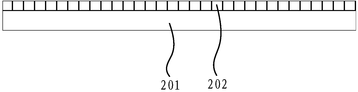
[0041] Step S21: providing a base substrate 201, such as figure 2 shown.

[0042] In order to ensure better performance of the product, it is preferable to perform initial cleaning on the base substrate 201 to remove impurity particles remaining on the surface of the base substrate during the production process.

[0043] The specific material of the provided base substrate 201 can be determined according to the actual situation. If the display device to be produced is non-flexible, the base substrate 201 is preferably a glass substrate. If a flexible or bendable display device needs to be produced, Then, the base substrate 201 may preferably be a flexible or bendable material such as a plastic film.

[0044] Step S22: forming a buffer layer 202 on the base substrate 201, such as image 3 shown.

[004...

Example Embodiment

[0120] Embodiment two

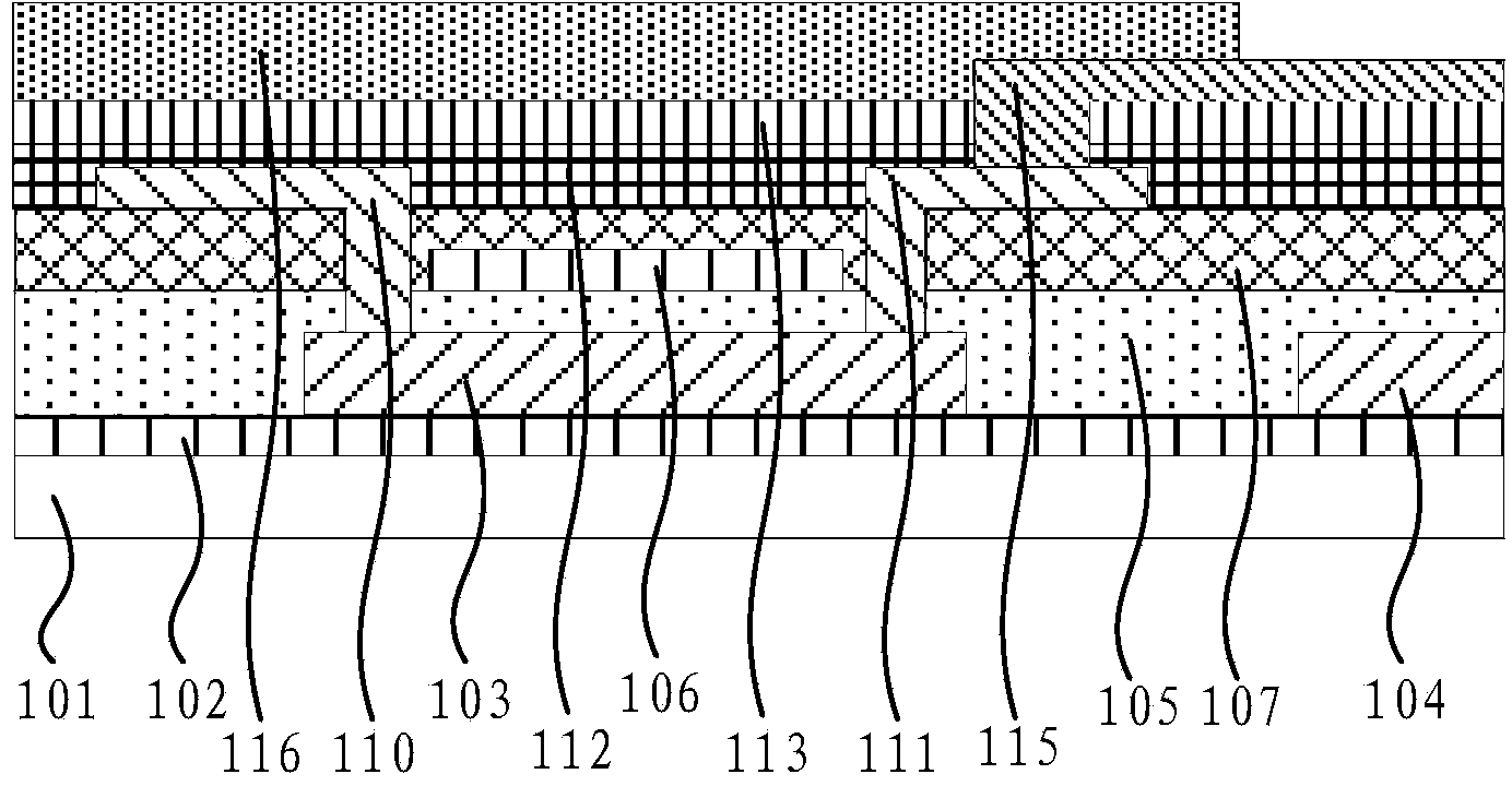
[0121] This embodiment provides an array substrate, such as Figure 13 As shown, the array substrate provided in this embodiment includes: an active layer 203 on the base substrate 201; a gate insulating layer 205 covering the active layer 203; Gate 206, source 207, drain 208, gate line and data line, gate line or data line are disconnected at the intersection of gate line and data line; cover gate 206, source 207, drain 208 , the passivation layer 209 of the gate line and the data line; the source contact hole, the drain contact hole and the bridge structure contact hole located inside the passivation layer 209 and the gate insulating layer 205, and the source contact hole exposes part of the source electrode 207 and part of the active layer 203, the drain contact hole exposes part of the drain electrode 208 and part of the active layer 203, and the bridge structure contact hole exposes part of the disconnected gate line or data line; the source locat...

Example Embodiment

[0134] Embodiment Three

[0135] Based on the second embodiment, this embodiment provides a display device, which includes the array substrate described in the second embodiment.

[0136] The display device provided in this embodiment can preferably be an OLED (Organic Light Emitting Diode, organic light emitting diode) display device, such as: AMOLED (Active Matrix Organic Light Emitting Diode, active matrix organic light emitting diode) display device; it can also be LCD (Liquid Crystal Display, liquid crystal display device), such as: IPS (In-Plane Switching, in-plane switching) type LCD, etc.

[0137] In the display device provided by this embodiment, the gate and the source and drain of the TFT are in the same film layer, so there is no parasitic capacitance between the gate and the source and drain, thereby improving the performance of the display device.

[0138] Moreover, since the array substrate of the display device in this embodiment can be fabricated using fewer ...


PUM

PropertyMeasurementUnit
Thicknessaaaaaaaaaa
Thicknessaaaaaaaaaa
Thicknessaaaaaaaaaa

Abstract

The invention provides an array substrate, a preparing method thereof and a display device, wherein the preparing method comprises the steps of: forming a pattern and a gate electrode insulating layer on a substrate, wherein the pattern comprises an active layer; forming a metal film on the gate electrode insulating layer, patterning the metal film through a primary composition process for forming the pattern which comprises a gate electrode, a source electrode, a drain electrode, a gate line and a data line; forming a passivation layer on the substrate; patterning the passivation layer through the primary composition process for forming a source electrode contact hole, a drain electrode contact hole and an over-bridge structure contact hole; and forming a transparent conductive film on the substrate, eliminating partial transparent conductive film through a film peeling process for forming a source electrode contact part, a drain electrode contact hole, a pixel electrode and an over-bridge structure. According to the preparing method, number of times in using the composition process is reduced. The array substrate has advantages of simple preparing process, high production efficiency and high yield rate.

Description

technical field [0001] The present invention relates to the field of display technology, in particular to an array substrate, a manufacturing method thereof, and a display device. Background technique [0002] The Active Matrix display device is a display device that uses thin film transistors (Thin Film Transistor, TFT for short) for pixel display driving. It has many advantages such as light and thin, low power consumption, low radiation, and low cost. The most mainstream display technology. [0003] Active matrix display devices all include a TFT array substrate. According to the different materials for the formation of the TFT active layer, the TFT array substrate can be divided into amorphous silicon (a-Si: H), low temperature polysilicon (Low Temperature Poly-Silicon, LTPS for short), high temperature polysilicon (High Temperature Poly-Silicon, HTPS for short), oxide semiconductor and other types. Among them, the LTPS TFT array substrate has become one of the researc...

Claims


Application Information

Patent Timeline
IPC IPC(8): H01L21/77H01L27/112G02F1/1362G02F1/1368H01L27/32
CPCG02F1/1368H01L27/1214H01L27/127H01L2021/775G02F1/136231H10K59/12G02F1/136227H01L29/41733H01L29/42384H01L27/124H01L27/1274H01L27/1288H01L27/1248H01L27/1255H01L29/66757H01L29/78675G02F1/13625H10K59/123H10K59/1213H01L21/77H01L27/12G02F1/134363G02F1/136286H01L21/26513H01L21/266H01L29/78618
Inventor 龙春平任章淳刘建宏
Owner BOE TECH GRP CO LTD
Why Eureka
Try Eureka