Double-gate p-channel mosfet with compressive strain film strain source and its preparation method

A technology of compressive strain and thin film, which is applied in the manufacture of semiconductor/solid-state devices, semiconductor devices, electrical components, etc., can solve the problems of poor thermal stability of GeSn materials, segregation of Sn atoms, etc., to reduce the effective mass of holes, conduct The effect of reducing on-resistance and improving hole mobility

Inactive Publication Date: 2017-03-01
CHONGQING UNIV
View PDF7 Cites 0 Cited by
  • Summary
  • Abstract
  • Description
  • Claims
  • Application Information

AI Technical Summary

Problems solved by technology

However, if the Sn component is too high, the thermal stability of the GeSn material will deteriorate, and the segregation of Sn atoms will easily occur.

Method used


Image

  • Double-gate p-channel mosfet with compressive strain film strain source and its preparation method
  • Double-gate p-channel mosfet with compressive strain film strain source and its preparation method
  • Double-gate p-channel mosfet with compressive strain film strain source and its preparation method

Examples


Embodiment Construction

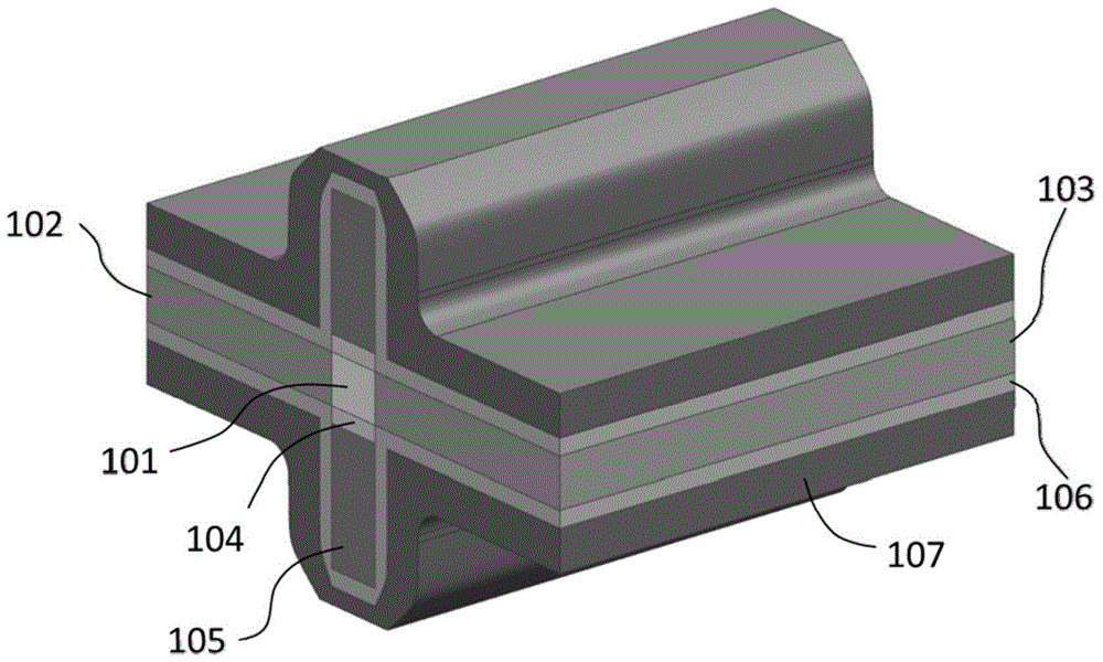
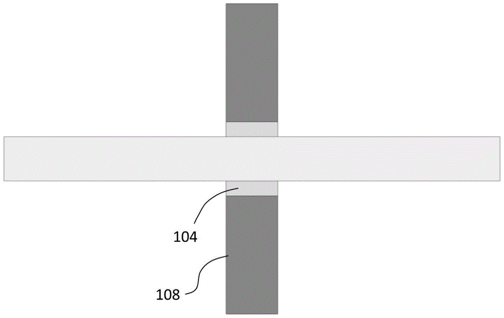
[0034] Embodiments of the present invention are described in detail below, examples of which are shown in the drawings, wherein the same or similar reference numerals designate the same or similar elements or elements having the same or similar functions throughout. The embodiments described below by referring to the figures are exemplary only for explaining the present invention and should not be construed as limiting the present invention.

[0035] In describing the present invention, it should be understood that the terms "longitudinal", "transverse", "upper", "lower", "front", "rear", "left", "right", "vertical", The orientations or positional relationships indicated by "horizontal", "top", "bottom", "inner", "outer", etc. are based on the orientations or positional relationships shown in the drawings, and are only for the convenience of describing the present invention and simplifying the description, rather than Nothing indicating or implying that a referenced device or ...


PUM


Abstract

The invention provides a double-gate p-channel MOSFET with a compression strain thin film strain source and a preparation method of the double-gate p-channel MOSFET with the compression strain thin film strain source. The MOSFET comprises a source region, a drain region, a conducting channel region, a gate dielectric layer, a grid electrode, an insulating dielectric layer and a compression strain thin film strain layer. The gate dielectric layer is formed on a first surface of a semiconductor material and located on the side face of a first conducting surface and the side face of a second conducting surface of the conducting channel region. The grid electrode is formed on the first surface of the semiconductor material and located on the side face of the gate dielectric layer. The insulating dielectric layer is formed on the side wall of the grid electrode, the side wall of a source electrode and the side wall of a drain electrode. The compression strain thin film strain layer is formed on the side wall of the insulating dielectric layer and used for leading compression strain in the channel direction into the conducting channel region. The surface of the MOSFET is covered with the compression strain thin film strain layer, and the large compression strain in the channel direction is led into the conducting channel region; as a result, effective mass of holes can be reduced, the migration rate of the holes is increased, the working current of the MOSFET is increased, and on-resistance is lowered.

Description

technical field [0001] The invention relates to the technical field of semiconductor design and manufacture, in particular to a double-gate p-channel MOSFET (metal oxide semiconductor field effect transistor, metal oxide semiconductor field effect transistor) with a compressive strain film strain source and a preparation method. Background technique [0002] With the rapid and in-depth development of integrated circuit technology, the increase of wafer size and the reduction of chip feature size can meet the requirements of miniaturization, high density, high speed, high reliability and system integration. According to the forecast of International Technology Roadmap for Semiconductors (ITRS) 2012, when the technology node of integrated circuits reaches below 10 nanometers, the strained Si material can no longer meet the needs, and it is necessary to introduce high-carrier mobility material MOSFET to improve Chip properties, such as Ge and GeSn. [0003] GeSn has a higher h...

Claims


Application Information

Patent Timeline
Patent Type & Authority Patents(China)
IPC IPC(8): H01L29/78H01L21/336
CPCH01L29/66477H01L29/7843
Inventor 刘艳韩根全赵斌张庆芳
Owner CHONGQING UNIV
Why Eureka
Try Eureka