
Eureka
For R&D, Eureka makes reading and utilizing patents & technical documents easy.
Eureka AIR
Designed for self-driven R&D workflows. Generate viable solutions, solve complex R&D challenges, empower your innovation with AI.

Eureka Materials
Designed for material experts only. Revolutionize your material R&D, from search, analyze, to developing new materials.

TechResearch
Generate reliable direction feasibility study reports for your R&D in just a few steps.

TechSeek
Discover and master advanced knowledge NOW. Basics, ideas, possibilities, all at once.

TechMind
As an expert in R&D Theories, TechMind can generates customized viable solutions instantly.

TechRisk
Analyze your overall solution with one click, know your potential R&D risks in advance.

TechMonitor
Get weekly tech updates, stay abreast of the latest tech innovations and key insights.
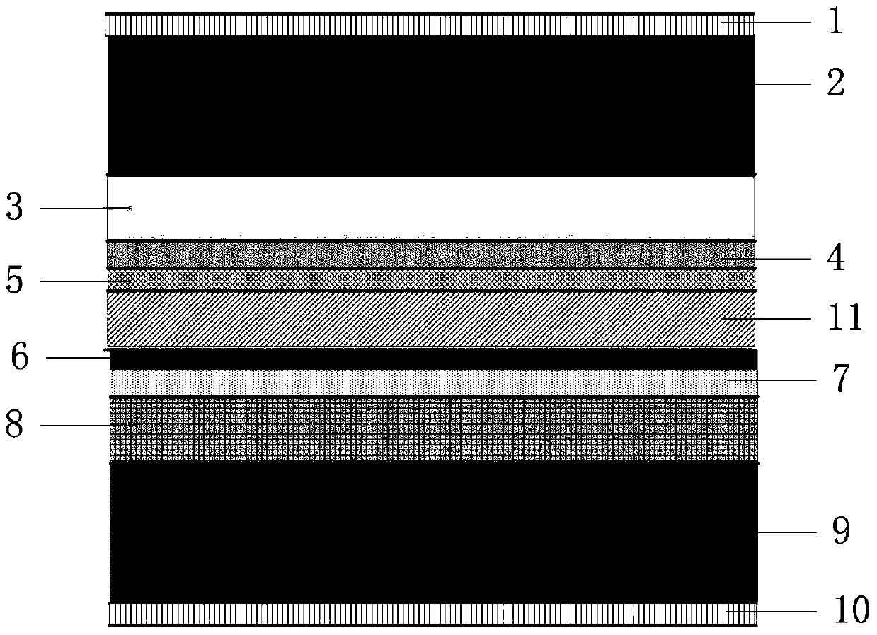
Series-connection sandwich-type epitaxy GaN PIN-type beta irradiation battery and preparation method
A sandwich type, epitaxy technology, applied in the field of microelectronics, can solve the problems of easy introduction of surface defects, low energy conversion rate, large leakage current of devices, etc., and achieve the effect of improving energy utilization rate, energy conversion rate, and working voltage.
- Summary
- Abstract
- Description
- Claims
- Application Information
AI Technical Summary
Problems solved by technology
Method used
Image

Examples
Embodiment 1
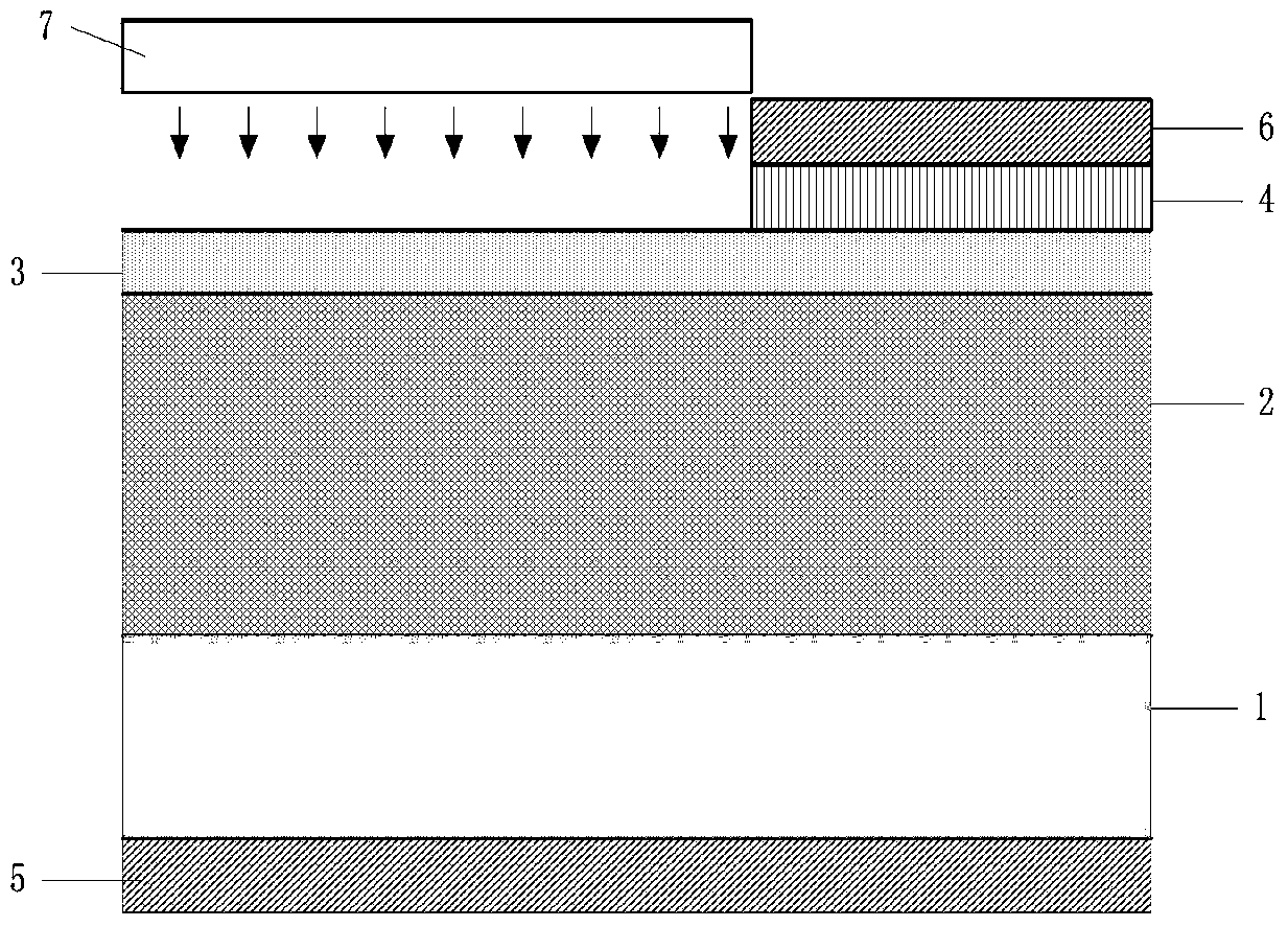
[0049] Embodiment 1, preparation sandwich radioactive source is Ni 63 , PIN-type β-irradiated cells with a thickness of β-radiation source layer of 4 μm in series sandwich epitaxial GaN.
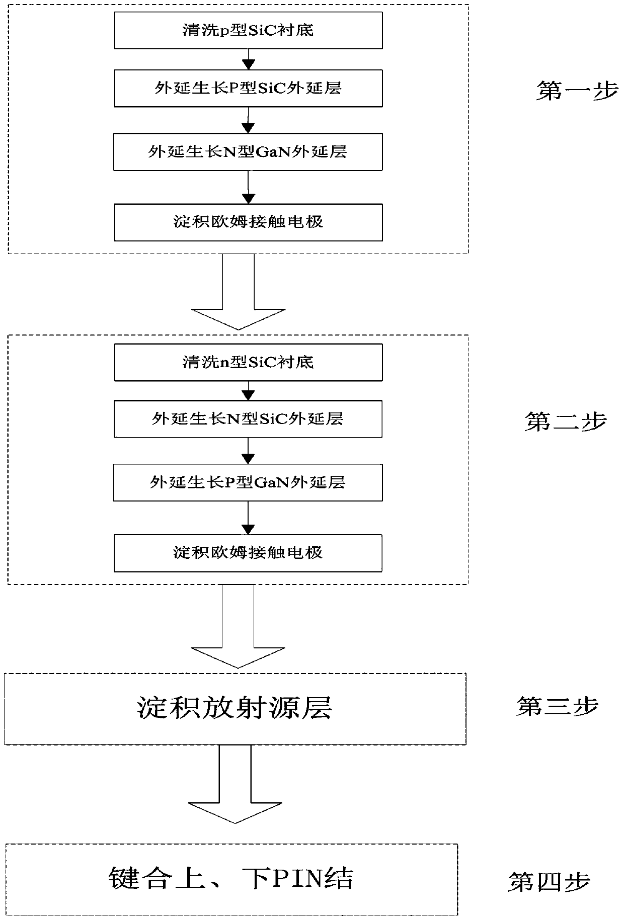
[0050] Step 1: Make the upper PIN knot.
[0051] (1a) Clean the p-type SiC substrate to remove surface contaminants:
[0052] (1a.1) Set the doping concentration to l.5x10 18 cm -3 Soak the p-type SiC substrate in NH4OH+H2O2 reagent for 10 minutes, take it out and dry it to remove the organic residue on the surface of the sample;
[0053] (1a.2) Soak the p-type SiC substrate after removing the surface organic residues with HCl+H2O2 reagent for 10 minutes, take it out and dry it to remove ionic pollutants.
[0054] (1b) Epitaxial growth of P-type SiC epitaxial layer:
[0055] An aluminum-doped P-type doped epitaxial layer is epitaxially grown on the cleaned p-type SiC substrate by chemical vapor deposition CVD. The process conditions are as follows: the epitaxy temperature is 1550°C, th...
Embodiment 2
[0079] Embodiment 2, preparation sandwich radioactive source is Ni 63 , PIN-type β-irradiated cells with a thickness of β-radiation source layer of 6 μm in series sandwich epitaxial GaN.
[0080] Step 1: Make the upper PIN knot.
[0081] 1a) cleaning the p-type SiC substrate to remove surface contaminants, the doping concentration of the p-type SiC substrate is 1.5×10 18 cm -3 :
[0082] This step is the same as step (1a) of Embodiment 1.
[0083] 1b) Epitaxial growth of P-type SiC epitaxial layer:
[0084] An aluminum-doped P-type SiC epitaxial layer is epitaxially grown on the cleaned p-type SiC substrate by chemical vapor deposition CVD. Under the conditions of epitaxy temperature of 1550°C, pressure of 100mbar, reaction gas of silane and propane, carrier gas of pure hydrogen, and impurity source of trimethylaluminum, the aluminum doping concentration is 3x10 15 cm -3 , a P-type SiC epitaxial layer with a thickness of 22 μm.
[0085] 1c) Epitaxial growth of N-type G...
Embodiment 3
[0103] Embodiment 3, preparation sandwich radioactive source is Pm 147 , PIN-type β-irradiated cells with tandem sandwich epitaxial GaN with a thickness of β-radiation source layer of 14 μm.
[0104] Step A: Make the upper PIN knot.
[0105] A1) cleaning p-type SiC substrate, to remove surface pollutants, the doping concentration of this p-type SiC substrate is 1.5×10 18 cm -3 .
[0106] This step is the same as step (1a) of Embodiment 1.
[0107] A2) Epitaxial growth of P-type SiC epitaxial layer: on the cleaned p-type SiC substrate, an aluminum-doped P-type doped epitaxial layer is epitaxially grown by chemical vapor deposition CVD. The process conditions are as follows: the epitaxy temperature is 1550°C, the pressure is 100mbar, the reaction gas is silane and propane, the carrier gas is pure hydrogen, the impurity source is trimethylaluminum, and the aluminum doping concentration is 4x10 15 cm -3 , a P-type SiC epitaxial layer with a thickness of 30 μm.
[0108] A3) ...
PUM
| Property | Measurement | Unit |
|---|---|---|
| Doping concentration | aaaaa | aaaaa |
| Doping concentration | aaaaa | aaaaa |
| Doping concentration | aaaaa | aaaaa |
Abstract
Description
Claims
Application Information
 - R&D Engineer
- R&D Manager
- IP Professional
- Industry Leading Data Capabilities
- Powerful AI technology
- Patent DNA Extraction
Browse by: Latest US Patents, China's latest patents, Technical Efficacy Thesaurus, Application Domain, Technology Topic, Popular Technical Reports.
© 2024 PatSnap. All rights reserved.Legal|Privacy policy|Modern Slavery Act Transparency Statement|Sitemap|About US| Contact US: help@patsnap.com