Epitaxy GaN parallel type PIN type alpha irradiation battery and manufacturing method thereof

A parallel battery technology, applied in the field of microelectronics, can solve the problems of easy introduction of surface defects, large device leakage current, low energy conversion rate, etc., to achieve improved energy collection rate, large band gap, and good radiation resistance Effect

Inactive Publication Date: 2014-09-17
XIDIAN UNIV
View PDF4 Cites 0 Cited by
  • Summary
  • Abstract
  • Description
  • Claims
  • Application Information

AI Technical Summary

Problems solved by technology

The substrate used in this structure is a P-type highly doped substrate, and the existing process of growing an epitaxial layer on the substrate is immature, so it is easy to introduce surface defects, the leakage current of the device is large, and the energy conversion rate is low.

Method used


Image

  • Epitaxy GaN parallel type PIN type alpha irradiation battery and manufacturing method thereof
  • Epitaxy GaN parallel type PIN type alpha irradiation battery and manufacturing method thereof
  • Epitaxy GaN parallel type PIN type alpha irradiation battery and manufacturing method thereof

Examples


Embodiment 1

[0042] Embodiment 1, preparation α radiation source is Am 241 , Parallel-connected PIN-type α-irradiated cells with epitaxial GaN with two trenches.

[0043] Step 1: Make the lower PIN knot.

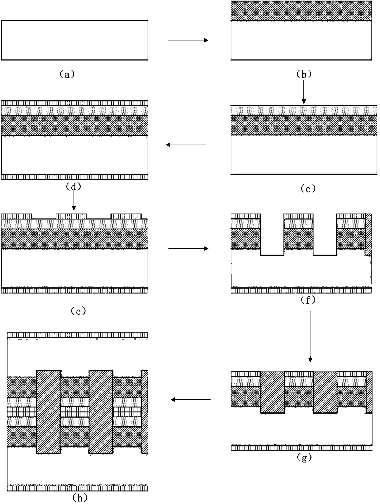
[0044] (1a) Clean the 4H-SiC sample to remove surface contaminants, such as image 3 (a) shown.

[0045] (1a.1) Set the doping concentration to lx10 18 cm -3 Highly doped n-type 4H-SiC substrate sample in NH 4 OH+H 2 o 2 Soak the sample in the reagent for 10 minutes, take it out and dry it to remove the organic residue on the surface of the sample;

[0046] (1a.2) Use HCl+H to remove the 4H-SiC sample after removing the surface organic residues 2 o 2 Soak the sample in the reagent for 10 minutes, take it out and dry it to remove ionic pollutants.

[0047] (1b) Epitaxial growth of N-type low-doped SiC epitaxial layer, such as image 3 (b) shown.

[0048] A nitrogen-doped N-type low-doped SiC epitaxial layer was epitaxially grown on the cleaned SiC sample by chemical vapor depo...

Embodiment 2

[0068] Embodiment 2, preparation α radiation source is Am 241 , Parallel-connected PIN-type α-irradiated cells of epitaxial GaN with seven trenches.

[0069] Step 1: Make the lower PIN knot.

[0070] 1a) Clean the 4H-SiC sample to remove surface contaminants such as image 3 (a).

[0071] This step is the same as step (1a) of Example 1.

[0072] 1b) Epitaxial growth of N-type low-doped SiC epitaxial layer, such as image 3 (b).

[0073] A nitrogen-doped N-type low-doped SiC epitaxial layer was epitaxially grown on the cleaned SiC sample by chemical vapor deposition CVD. The process conditions are: epitaxy temperature is 1550°C, pressure is 100mbar, reaction gas is silane and propane, carrier gas is pure hydrogen, magazine source is liquid nitrogen, and nitrogen doping concentration is 1.5x10 15 cm -3 , growth of an N-type low-doped SiC epitaxial layer with a thickness of 8 μm.

[0074] 1c) Epitaxial growth of P-type highly doped GaN epitaxial layer, such as image 3 (c)...

Embodiment 3

[0090] Embodiment 3, preparation α radiation source is Pu 238 , Parallel-connected PIN-type α-irradiated cells of epitaxial GaN with 15 trenches.

[0091] Step A: Make the upper PIN knot.

[0092] (A1) Clean the 4H-SiC sample to remove surface contaminants, such as image 3 (a).

[0093] This step is the same as step (1a) of Example 1.

[0094] (A2) A nitrogen-doped N-type low-doped SiC epitaxial layer is epitaxially grown on the cleaned SiC sample by chemical vapor deposition CVD. The process conditions are as follows: the epitaxy temperature is 1550°C, the pressure is 100mbar, the reaction gas is silane and propane, the carrier gas is pure hydrogen, and the magazine source is liquid nitrogen. A nitrogen doping concentration of 2x10 15 cm -3 , a N-type low-doped SiC epitaxial layer with a thickness of 10 μm such as image 3 (b).

[0095] (A3) Put the sample after growing the N-type low-doped SiC epitaxial layer into the chemical vapor deposition CVD furnace. 2 Heated...


PUM


Abstract

The invention discloses an epitaxy GaN parallel type PIN type alpha irradiation battery and a manufacturing method of the epitaxy GaN parallel type PIN type alpha irradiation battery. The epitaxy GaN parallel type PIN type alpha irradiation battery mainly solves the problem that the current nuclear battery energy conversion rate and output power are low and comprises an upper PIN node, a lower PIN node and alpha irradiation sources, the upper PIN node and the lower PIN node are in parallel connection, the lower PIN node sequentially comprises an N-type ohmic contact electrode, an N-type highly-doped 4H-SiC substrate, an N-type lowly-doped SiC epitaxial layer, a P-type highly-doped GaN epitaxial layer and a P-type ohmic contact electrode from bottom to top, and the bottom-to-top structural distribution of the upper PIN node is the same as that of the lower PIN node. A plurality of grooves are formed in each PIN node, the alpha irradiation sources are arranged in the grooves respectively, the two PIN nodes are in contact through the P-type ohmic contact electrode, and the upper grooves and the lower grooves are in mirror symmetry and are communicated. The epitaxy GaN parallel type PIN type alpha irradiation battery has the advantages that the contact area between the irradiation sources and a semiconductor is large, the utilization and the energy collecting rate of the nuclear raw materials are high, and the output voltage of the battery is high, and a microcircuit can be constantly powered up.

Description

technical field [0001] The invention belongs to the field of microelectronics, and relates to a semiconductor device structure and a preparation method, in particular to a silicon carbide-based epitaxial GaN parallel-connected PIN type α irradiation battery and a preparation method thereof, which can be used for micro-circuits such as micro-nano electromechanical systems And aerospace, deep sea, polar regions and other occasions that require long-term power supply and are unattended. technical background [0002] With people's demand for low power consumption, long life, high reliability and small size power supply equipment, as well as concerns about nuclear waste disposal, micronuclear batteries have become more and more popular. Due to its outstanding characteristics, micronuclear batteries can be used to solve the long-term power supply problems of micropipe robots, implanted microsystems, wireless sensor node networks, artificial cardiac pacemakers, and portable mobile ...

Claims


Application Information

Patent Timeline
Patent Type & Authority Applications(China)
IPC IPC(8): G21H1/06
Inventor 郭辉赵亚秋王悦湖张艺蒙张玉明
Owner XIDIAN UNIV
Why Eureka
Try Eureka