A double-layer gate dielectric thin film transistor with electrochromic properties

An electrochromic and dielectric thin film technology, which is applied in the direction of transistors, circuits, electrical components, etc., can solve the problems of poor uniformity of polysilicon thin film transistors, difficulty in providing driving current for light-emitting devices, and low carrier mobility, so as to improve the overall Performance, effect suitable for mass production

Active Publication Date: 2017-06-27
江阴智产汇知识产权运营有限公司
View PDF3 Cites 0 Cited by
  • Summary
  • Abstract
  • Description
  • Claims
  • Application Information

AI Technical Summary

Problems solved by technology

[0002] A thin film transistor is a field effect device composed of a semiconductor thin film, a thin film electrode and a gate insulating layer. It uses an electric field to regulate the Fermi level position of the semiconductor material and then regulates its conductivity. Therefore, it can be used as an active matrix organic light-emitting diode and thin film The core components of drive circuits such as transistors and liquid crystal displays; the carrier mobility of traditional amorphous silicon films is low, and it is difficult to provide large drive currents required by light-emitting devices; polysilicon films have intercrystalline boundaries, and the grain size varies First-class problems lead to poor uniformity of polysilicon thin film transistors and high manufacturing costs; organic transistor technology is still immature, and its carrier mobility, stability and other issues need to be further considered; in recent years, wide bandgap oxide semiconductor thin film transistors have High mobility, low temperature process, good compatibility with flexible substrates, large-scale production, low cost and other advantages, have broad application prospects in smart cards, electronic tags, electronic paper, memory, sensors and active matrix displays, etc. Therefore, it has aroused great research interest of experts at home and abroad. Wide bandgap oxide semiconductor thin film transistors usually require a relatively large operating voltage to obtain high output current and high mobility; One of the research hotspots; low-voltage oxide thin film transistors can effectively reduce the power loss of devices and circuits, and have potential application value in the field of portable microelectronics

Method used


Image

  • A double-layer gate dielectric thin film transistor with electrochromic properties
  • A double-layer gate dielectric thin film transistor with electrochromic properties

Examples


preparation example Construction

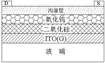
[0019] A preparation method of an electrochromic double-layer gate dielectric thin film transistor of the present invention comprises the following steps:

[0020] 1. Gate electrode preparation;

[0021] 2. Preparation of double-layer gate dielectric layer;

[0022] 3. Trench production;

[0023] 4. Masking, preparation of source (S) and drain (D).

Embodiment 1

[0025] 1. Clean the ITO glass substrate.

[0026] 2. The silicon dioxide proton conductor film was prepared by plasma chemical vapor deposition technology; the reaction gases used were silane and phosphine, and the concentration ratio was 9:1; argon gas was used for ignition; the oxygen flow rate used was 10 sccm; the radio frequency power used was 100W; The deposition pressure is 30 Pa; the temperature used is room temperature; and the thickness is 500 nm.

[0027] 3. The tungsten oxide film was prepared by sputtering. The target material used was a tungsten target with a concentration of 99.99%. Argon was used for ignition, the oxygen flow rate used was 14sccm, the radio frequency power was 100W, the deposition pressure was 0.1Pa, and the thickness was 300nm.

[0028] 4. Using magnetron sputtering technology, IZO is used as a target material, at room temperature, the reaction pressure is set to 1Pa, and the radio frequency power is set to 100W to prepare a channel layer with...

Embodiment 2

[0031] 1. Clean the common glass substrate.

[0032] 2. Using magnetron sputtering technology, using ITO as the target material, at room temperature, set the reaction pressure to 1Pa and the radio frequency power to 100W to prepare a gate electrode with a thickness of 80nm.

[0033] 3. The silicon dioxide proton conductor film was prepared by plasma chemical vapor deposition technology; the reaction gases used were silane and phosphine, the concentration ratio was 9:1; argon gas was used for ignition; the oxygen flow rate used was 10 sccm; the radio frequency power used was 200W; The deposition pressure is 10 Pa; the temperature used is room temperature; and the thickness is 1000 nm.

[0034] 4. The tungsten oxide film was prepared by sputtering. The target material used was a tungsten target with a concentration of 99.99%. Argon gas was used for ignition, the oxygen flow rate used was 14 sccm, the radio frequency power was 100W, the deposition pressure was 0.1Pa, and the thic...


PUM


Abstract

The invention relates to the technical field of semiconductor thin film transistors and electrochromism electronic devices, in particular to a double-layer gate dielectric thin film transistor with the electrochromism characteristic and a manufacturing method of the double-layer gate dielectric thin film transistor. According to the electrochromism principle, when voltage is applied to the transistor, tungsten oxide in the transistor is excited to change color, the electrochromism device is designed according to the phenomenon that the light-transmittance characteristic of the transistor changes, the silicon dioxide with the proton conductive characteristic serves as an ion storage layer, protons needed by color change are provided for electrochromism, the tungsten oxide and the silicon dioxide both serve as the grate dielectric of the thin film transistor, and the double-layer gate dielectric thin film transistor with the electrochromism characteristic can be manufactured.

Description

technical field [0001] The invention relates to the technical field of semiconductor thin film transistors and electrochromic electronic devices, in particular to an electrochromic double-layer gate dielectric thin film transistor and a manufacturing method thereof. Background technique [0002] A thin film transistor is a field effect device composed of a semiconductor thin film, a thin film electrode and a gate insulating layer. It uses an electric field to regulate the Fermi level position of the semiconductor material and then regulates its conductivity. Therefore, it can be used as an active matrix organic light-emitting diode and thin film The core components of drive circuits such as transistors and liquid crystal displays; the carrier mobility of traditional amorphous silicon films is low, and it is difficult to provide large drive currents required by light-emitting devices; polysilicon films have intercrystalline boundaries, and the grain size varies First-class pr...

Claims


Application Information

Patent Timeline
Patent Type & Authority Patents(China)
IPC IPC(8): H01L29/786H01L29/51
CPCH01L29/511H01L29/517H01L29/7869
Inventor 郭立强丁建宁凌智勇程广贵张忠强
Owner 江阴智产汇知识产权运营有限公司
Why Eureka
Try Eureka