Surface plasmon polariton-enhanced photoelectric detector based on MIM (Metal Injection Molding) structure

A surface plasmon and photodetector technology, applied in the field of detection and sensing, can solve problems such as unfavorable integration and reduction of raw material costs, insufficient spectral response range of detectors, toxicity of photoelectric sensitive materials, etc., and achieves less consumables. , to stimulate the effect of high efficiency and easy production

Inactive Publication Date: 2014-09-24
SUZHOU UNIV
View PDF2 Cites 24 Cited by
  • Summary
  • Abstract
  • Description
  • Claims
  • Application Information

AI Technical Summary

Problems solved by technology

[0006] For traditional semiconductor detectors, the existing problems in the current theory and technology are: (1) The designed photodetector is relatively large in size, which is not conducive to integration and reduction of raw material cost

Method used


Image

  • Surface plasmon polariton-enhanced photoelectric detector based on MIM (Metal Injection Molding) structure
  • Surface plasmon polariton-enhanced photoelectric detector based on MIM (Metal Injection Molding) structure
  • Surface plasmon polariton-enhanced photoelectric detector based on MIM (Metal Injection Molding) structure

Examples


Embodiment 1

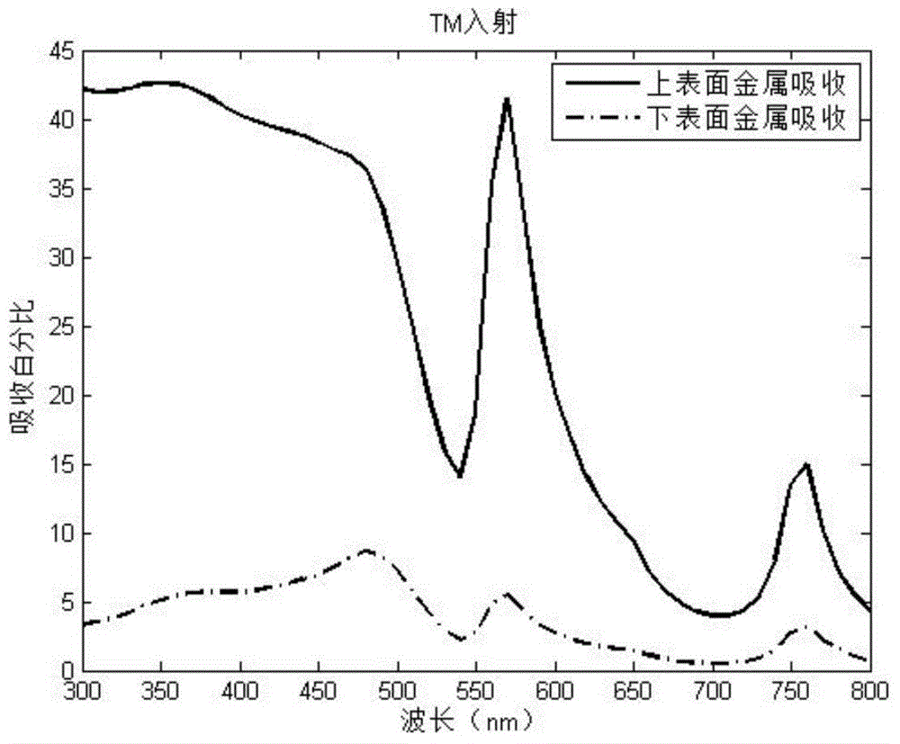
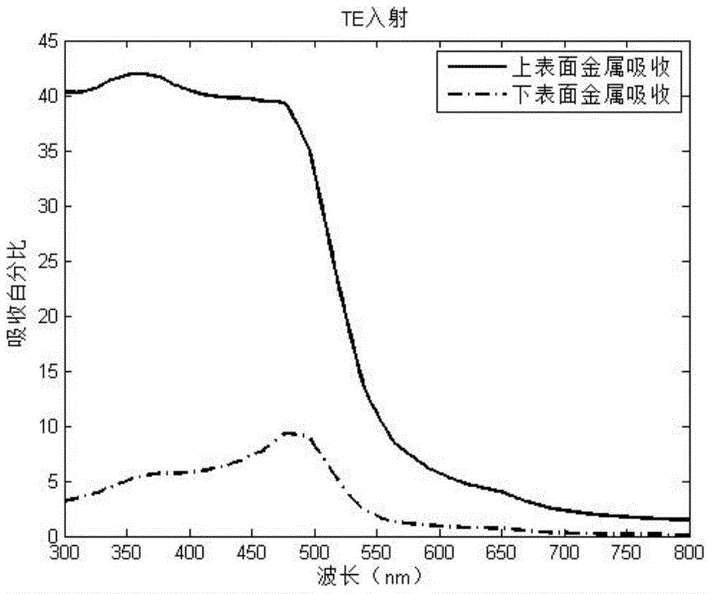
[0039] Embodiment 1: The structural parameters of the present invention are obtained by solving the electromagnetic field and using finite element algorithm simulation and optimization. The specific light absorption characteristics of the structure will be given in the accompanying drawings.

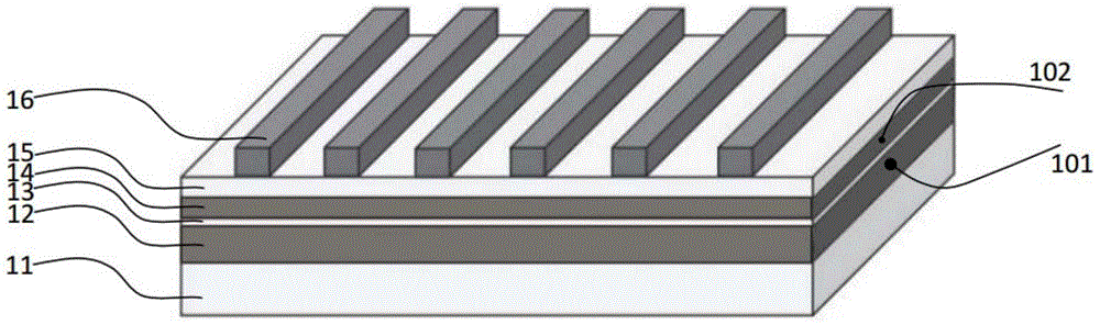
[0040] Combine figure 1 As shown, the surface plasmon-enhanced photodetector based on the MIM structure provided by this embodiment uses a substrate 11 (the material is quartz, the thickness is 1000 μm, and the thickness is generally thicker, taking practical operation as the starting point) , The lower metal film layer 12 (material is gold, thickness is 50nm), the lower dielectric spacer 13 (material is alumina, thickness is 3nm), upper metal film layer 14 (material is Gold, thickness 20nm), upper dielectric spacer 15 (material is silicon dioxide, thickness 30nm) and metal grating layer 16 (material is gold, thickness is 50nm, period is 500nm, duty cycle is 0.36), and includes The upper an...

Embodiment 2

[0051] Example 2: See the structure figure 1 It is the same as Embodiment 1, but the difference is that the period of the metal grating is changed from 500 nm in Embodiment 1 to 800 nm, that is, the duty cycle is still 0.3, and the thickness of the metal grating is 50 nm. Through the finite element method simulation, the response of the upper and lower metal film layers 14, 12 to the spectrum can be obtained. As attached Image 6 As shown, by adjusting the period, duty ratio, and thickness of the metal grating, the resonance wavelength of the surface plasmon is changed, which affects the difference in the response of the device to light in different spectral ranges. For this embodiment, from the attached Image 6 It can also be seen that at a wavelength of 1350 to 1550 nm, the upper and lower metal film layers 14, 12 have a large difference in light absorption, so this structure can be used to detect the subtle changes of incident photons in the above-mentioned wavelength range....

Embodiment 3

[0052] Example 3: See for its structure figure 1 It is the same as Embodiment 1, but the difference is that the period of the metal grating is changed from 500 nm in Embodiment 1 to 1000 nm, that is, the duty ratio is still 0.3, and the thickness of the metal grating is 50 nm. Through the finite element method simulation, the response of the upper and lower metal film layers 14, 12 to the spectrum can be obtained. As attached Figure 7 As shown, by adjusting the period, duty ratio, and thickness of the metal grating, the resonance wavelength of the surface plasmon is changed, which affects the difference in the response of the device to light in different spectral ranges. For this embodiment, from the attached Figure 7 It can be seen that at the wavelength of 1600 to 1900 nm, the upper and lower metal film layers 14, 12 have a relatively large difference in light absorption, so this structure can be used to detect the subtle changes of incident photons in the above wavelength...


PUM

PropertyMeasurementUnit
Thicknessaaaaaaaaaa
Thicknessaaaaaaaaaa
Thicknessaaaaaaaaaa

Abstract

The invention discloses a surface plasmon polariton-enhanced photoelectric detector based on an MIM (Metal Injection Molding) structure. The photoelectric detector comprises a substrate, and is characterized in that a lower metal film layer, a lower dielectric isolating layer, an upper metal film layer, an upper dielectric isolating layer and a metal grating layer are formed in sequence on the substrate from top to bottom. The surface plasmon polariton-enhanced photoelectric detector further comprises an upper metal film layer electrode lead, a lower metal film layer electrode lead, and a detector output port which is connected to the upper and lower metal film layers respectively. In the design, the local light trapping effect of a grating layer is achieved through the metal optical grating layer serving as a core, and an electron current tunneling effect is caused by remarkable difference between the light absorption of the upper and lower metal film layers. The photoelectric detector has the characteristics of small size (nanoscale), small number of consumables, simple structure, easiness in machining, wide spectral response, large detection angle and the like.

Description

Technical field [0001] The invention relates to a photodetector enhanced by surface plasmons based on a MIM structure, belonging to the technical field of detection and sensing. Background technique [0002] Converting incident photons into electrons is the main working process of photodetector devices. In the development process of modern photodetector devices, the volume of the devices is getting smaller and smaller, and the raw materials used are also developing in the direction of wide sources and non-toxicity. The sensitivity and responsiveness of the camera are gradually improving. Traditional photodetecting devices use semiconductor materials to illuminate, thereby generating carriers, and detecting the intensity of incident light by collecting photogenerated carriers to generate photocurrent. [0003] In the current mainstream photodetectors, although the thickness of semiconductor materials can be reduced to the order of micrometers, there are still many limitations in th...

Claims


Application Information

Patent Timeline
IPC IPC(8): H01L31/09
CPCH01L31/102H01L31/022408
Inventor 李孝峰吴凯吴绍龙杨阵海李珂
Owner SUZHOU UNIV
Why Eureka
Try Eureka