A kind of high-adhesion infrared metal reflective film and preparation method thereof
A technology of metal reflection and high adhesion, applied in metal layered products, chemical instruments and methods, metal material coating processes, etc. peeling off and other problems, to achieve the effect of improving moisture resistance and anti-friction performance, good surface mechanical strength, and improving film quality
- Summary
- Abstract
- Description
- Claims
- Application Information
AI Technical Summary
Problems solved by technology
Method used
Image
Examples
Embodiment 1
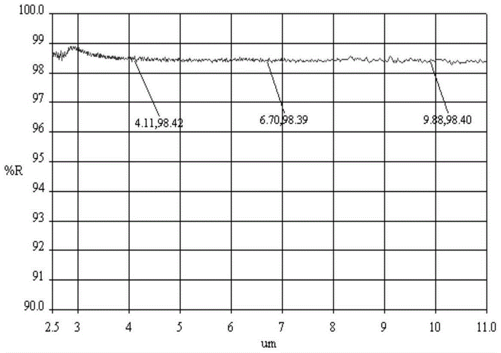
[0038] A medium-wave and long-wave infrared high-reflection film, the substrate material is single crystal silicon, and the size is 110×180×14mm. The technical requirements are as follows: The angle of incidence is 45°. Coating samples pass the adhesion and moderate friction test specified in GJB2485-1995 at one time.
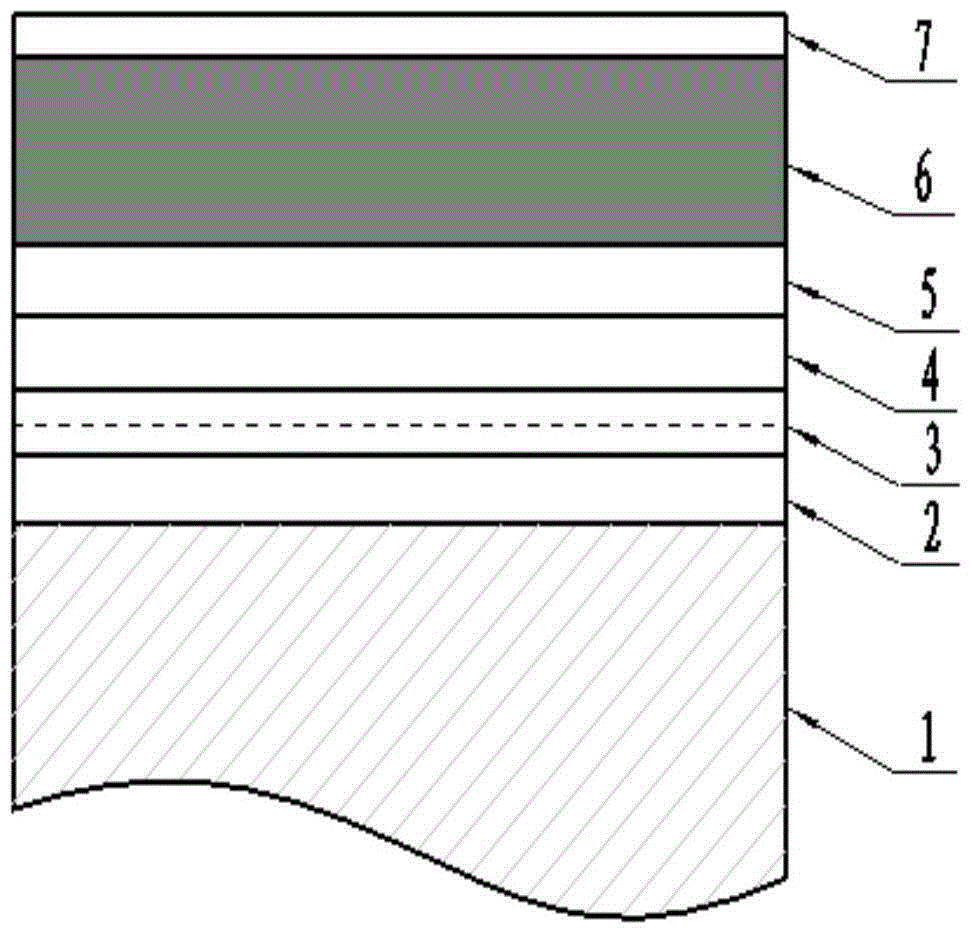
[0039] First of all, according to the above technical requirements, the optimal design of the film structure is carried out, and the results are as follows:
[0040] Sub / aCr / bM / cAu / dZnS / eYF 3 / fZnS / gTa 2 o 5 / Air
[0041] Wherein, a-f are the physical thickness of the film layer, M is the occlusal bonding layer composed of the ultra-thin chromium layer and the ultra-thin gold layer, and the physical thicknesses are 3.0nm and 5.5nm respectively. Other thicknesses are: a-30nm; c-130nm; d-18nm; e-125nm; f-60nm, g-20nm.
[0042] The specific implementation of the preparation process is as follows:
[0043] (1) Preparation: First, roughly wipe it with a spe...
Embodiment 2
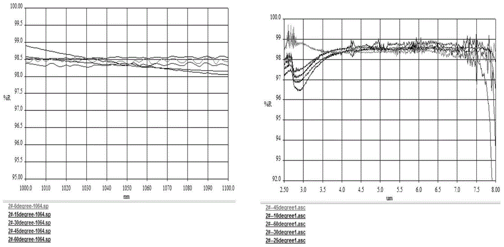
[0054] A laser / infrared dual-band high-reflection film, the substrate material is K9 glass, and the size is 100×140×12mm. The technical requirements are as follows: The incident angle is 10°~60°. Coating samples must pass the adhesion and moderate friction test specified in GJB2485-1995, and the threshold level of anti-laser damage is greater than 300MW / cm 2 .
[0055] First of all, according to the above technical requirements, the optimal design of the film structure is carried out, and the results are as follows:
[0056] Sub|aCr / bM / cAg / dAl 2 o 3 / eSiO 2 / fO 2 / gSiO 2 / TiO 2 / iTa 2 o 5 / Air
[0057] Wherein, a-f are the physical thickness of the film layer, M is the occlusal bonding layer composed of the ultra-thin copper layer and the ultra-thin silver layer, and the physical thicknesses are 8.5nm and 13.0nm respectively. Other thicknesses are: a-30nm; c-130nm; d-35nm; e-28nm; f-71.8nm; g-53.9nm; h-54.2nm; i-20nm.
[0058] The specific implementation of the p...
PUM
| Property | Measurement | Unit |
|---|---|---|
| thickness | aaaaa | aaaaa |
| thickness | aaaaa | aaaaa |
| thickness | aaaaa | aaaaa |
Abstract
Description
Claims
Application Information


