Binary blazed grating coupler and application thereof on silicon-based mixed integration photodetector

A technology of blazed gratings and photodetectors, applied in the coupling of optical waveguides, light guides, optics, etc., to achieve the effects of simple device structure, high coupling efficiency, and small volume

Inactive Publication Date: 2014-10-08
TIANJIN POLYTECHNIC UNIV
View PDF2 Cites 18 Cited by
  • Summary
  • Abstract
  • Description
  • Claims
  • Application Information

AI Technical Summary

Problems solved by technology

[0004] The purpose of the present invention is to solve the optical coupling problem between the SOI silicon nanowire waveguide and the InGaAs / InP photodetector in the arrayed waveguide grating demodulation integrated microsystem, to provide a binary blazed grating coupler, especially to provide an application A binary blazed grating coupler structure with high coupling efficiency, wide bandwidth, and simple process fabrication between silicon-based hybrid integrated photodetectors

Method used


Image

  • Binary blazed grating coupler and application thereof on silicon-based mixed integration photodetector
  • Binary blazed grating coupler and application thereof on silicon-based mixed integration photodetector
  • Binary blazed grating coupler and application thereof on silicon-based mixed integration photodetector

Examples


Embodiment Construction

[0031] The best embodiment of the present invention will be described in detail below in conjunction with technical solutions.

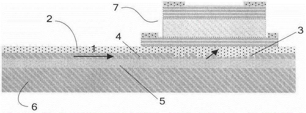
[0032] The purpose of the present invention is to solve the optical coupling problem between the SOI silicon nanowire waveguide and the InGaAs / InP photodetector in the arrayed waveguide grating demodulation integrated microsystem, and provide a binary blazed grating coupler whose structure mainly includes a silicon substrate bottom, confinement, waveguide and grating layers. The input light from the optical fiber or semiconductor laser is input from the waveguide layer, and the light is coupled into the optical fiber or photodetector above the grating under the action of grating diffraction. The specific implementation steps are:

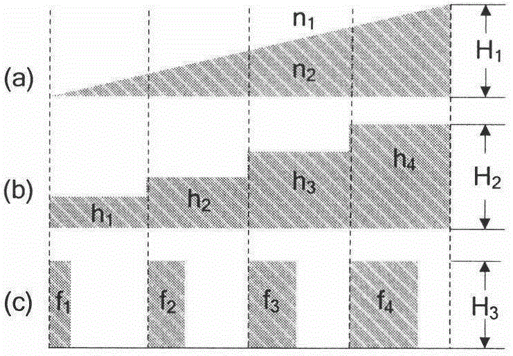
[0033] 1. Design of binary blazed grating coupler structure

[0034] The blazed grating can blaze the diffracted light to a certain diffraction order, which greatly improves the diffraction efficiency of the grating. Th...


PUM


Abstract

The invention provides a binary blazed grating coupler. The coupler is made of an SOI material and comprises a silicon substrate, a limiting layer, a waveguide layer and a grating layer. The grating layer is a binary blazed grating, the binary blazed grating is a one-dimensional binary blazed grating or a two-dimensional binary blazed grating, and the binary blazed grating coupler is simple in structure, convenient to manufacture, small in size and compatible with a standard CMOS process and achieves a coupling output function high in coupling efficiency and wide in bandwidth. By bonding a photodetector made of an III-V material to an SOI wafer, a silicon-based mixed integration photodetector with a grating coupling function is achieved; the silicon-based mixed integration photodetector is applied to an array waveguide grating demodulation integration microsystem, and the optical coupling problem between an SOI silicon nanowire waveguide in the array waveguide grating demodulation integration microsystem and an InGaAs/InP photodetector is effectively solved.

Description

technical field [0001] The invention relates to a coupling structure of an optical waveguide, in particular to a binary blazed grating coupler, which belongs to the field of optoelectronic integration. Background technique [0002] With the progress of society and the development of productivity, the size of integrated circuits will become smaller and smaller, and the speed of information transmission will be higher and higher, but the development of traditional microelectronics technology has approached its limit, making it an obstacle to the continued development of integrated circuits. a bottleneck in its development. Therefore, new devices, new interconnection methods and new integration methods must be developed to meet high-density data communication and high-speed data processing. As one of the most promising technologies to break this bottleneck, silicon-based optical devices have gradually been paid attention to, which makes it possible to further compress the devi...

Claims


Application Information

Patent Timeline
Patent Type & Authority Applications(China)
IPC IPC(8): G02B6/124G02B6/34G02B6/42
Inventor 李鸿强刘宇崔贝贝周文骞
Owner TIANJIN POLYTECHNIC UNIV
Why Eureka
Try Eureka