Antireflective film for solar cell piece and manufacturing method thereof
A solar cell sheet and manufacturing method technology, applied in the field of solar energy utilization, can solve problems such as poor anti-reflection effect, achieve the effects of improving short-circuit current, uniform appearance and color, and improving photoelectric conversion efficiency
- Summary
- Abstract
- Description
- Claims
- Application Information
AI Technical Summary
Problems solved by technology
Method used
Image
Examples
Embodiment 1
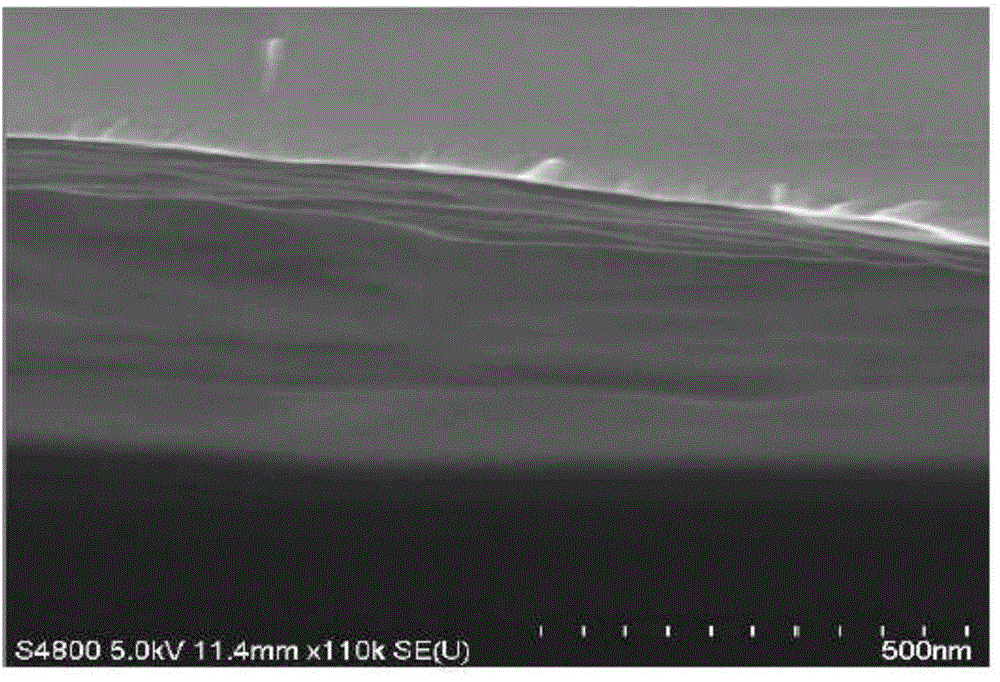
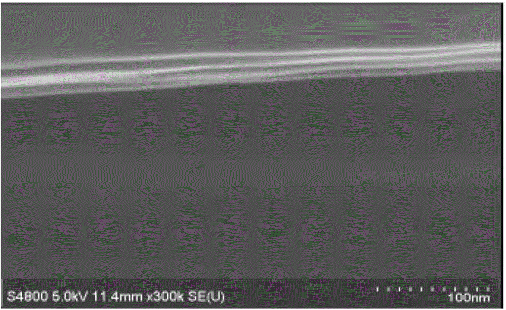
[0066] Using a domestic plasma enhanced chemical vapor deposition instrument (model: M82200-3 / UM), deposit the first layer of silicon nitride film on the surface of a clean and dry metallurgical polysilicon wafer at a temperature of 460°C, a pressure of 193Pa, and an ammonia gas flow rate of 3000sccm , the silane flow rate is 1000sccm, the deposition power is 4000W, and the duration is 100s to obtain the first silicon nitride film with a thickness of 24-26nm and a refractive index of 2.5-2.6;
[0067] Continuously deposit the second layer of silicon nitride film on the first layer of silicon nitride film, the temperature is 460°C, the pressure is 187Pa, the flow rate of ammonia gas is 3429sccm, the flow rate of silane is 571sccm, the deposition power is 4000W, and the duration is 70-90s to obtain a second layer of silicon nitride thin film with a thickness of 15-20 nm and a refractive index of 2.3-2.4;
[0068] Continuously deposit the third layer of silicon nitride film on th...
Embodiment 2
[0072] Using a domestic plasma enhanced chemical vapor deposition instrument (model: M82200-3 / UM), deposit the first layer of silicon nitride film on the surface of a clean and dry metallurgical polysilicon wafer at a temperature of 460°C, a pressure of 195Pa, and an ammonia flow rate of 3010sccm , the silane flow rate is 1003sccm, the deposition power is 2500W, and the duration is 100s to obtain the first layer of silicon nitride film with a thickness of 30nm and a refractive index of 2.7;
[0073] Adjust the deposition power to 0, maintain the pressure at 180-190Pa, stop feeding the reaction gas, and maintain this state for 5-10 seconds, and then start to deposit the second layer of silicon nitride film on the first layer of silicon nitride film , the temperature is 460°C, the pressure is 186Pa, the flow rate of ammonia gas is 3439 sccm, the flow rate of silane gas is 573 sccm, the deposition power is 2500W, and the duration is 90s to obtain a second layer of silicon nitride ...
PUM
| Property | Measurement | Unit |
|---|---|---|
| thickness | aaaaa | aaaaa |
| thickness | aaaaa | aaaaa |
| thickness | aaaaa | aaaaa |
Abstract
Description
Claims
Application Information


