Gallium-nitride transistor employing gap-type composite passivation medium and manufacturing method

A manufacturing method and gap-type technology, applied in semiconductor/solid-state device manufacturing, semiconductor devices, electrical components, etc., can solve the problems of device reliability failure, increase leakage current, etc., achieve reduced gate leakage, good effect, and simple process Effect

Active Publication Date: 2018-10-23
XIAMEN SANAN INTEGRATED CIRCUIT
View PDF4 Cites 4 Cited by
  • Summary
  • Abstract
  • Description
  • Claims
  • Application Information

AI Technical Summary

Problems solved by technology

However, the shallow-level trap states introduced after the deposition of silicon nitride become channels for device surface leakage, thereby increasing the gate (G) leakage current of the device, such as figure 2 As shown, this exposes the device to reliability failures

Method used


Image

  • Gallium-nitride transistor employing gap-type composite passivation medium and manufacturing method
  • Gallium-nitride transistor employing gap-type composite passivation medium and manufacturing method
  • Gallium-nitride transistor employing gap-type composite passivation medium and manufacturing method

Examples


Embodiment 1

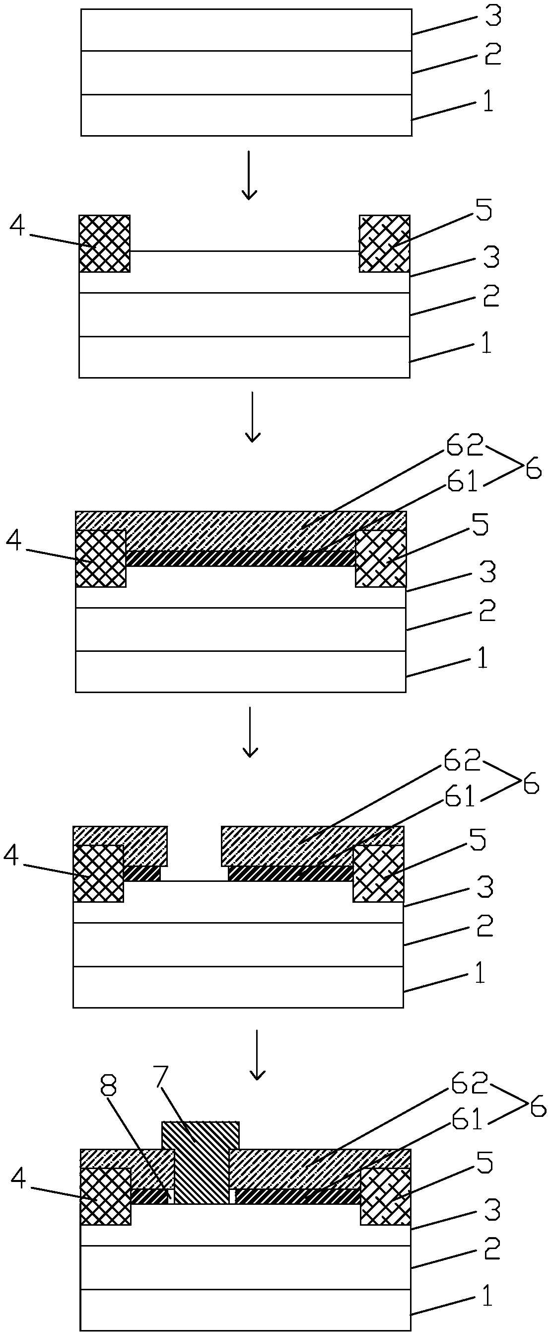
[0029] refer to figure 1 , the production method of this embodiment is as follows:

[0030] 1) An epitaxial layer is provided, and the epitaxial layer includes a substrate 1 , a gallium nitride layer 2 and a barrier layer 3 sequentially stacked from bottom to top. The substrate 1 may be silicon (Si), silicon carbide (SiC), or sapphire (Saphhire), and the barrier layer 3 may be aluminum gallium nitride.

[0031] 2) The isolation region is formed by mesa isolation or ion implantation planar isolation technology, and the source electrode 4 and the drain electrode 5 in ohmic contact with the barrier layer 3 are formed by conventional methods;

[0032] 3) Deposit SiN on the surface of the barrier layer 3 by PECVD after cleaning x For the dielectric, the lower dielectric layer 61 is first formed by using the growth condition with higher Si content, and then the upper dielectric layer 62 is formed by using the growth condition with higher N content. The lower dielectric layer 61 an...

Embodiment 2

[0037] The production method of this embodiment is as follows:

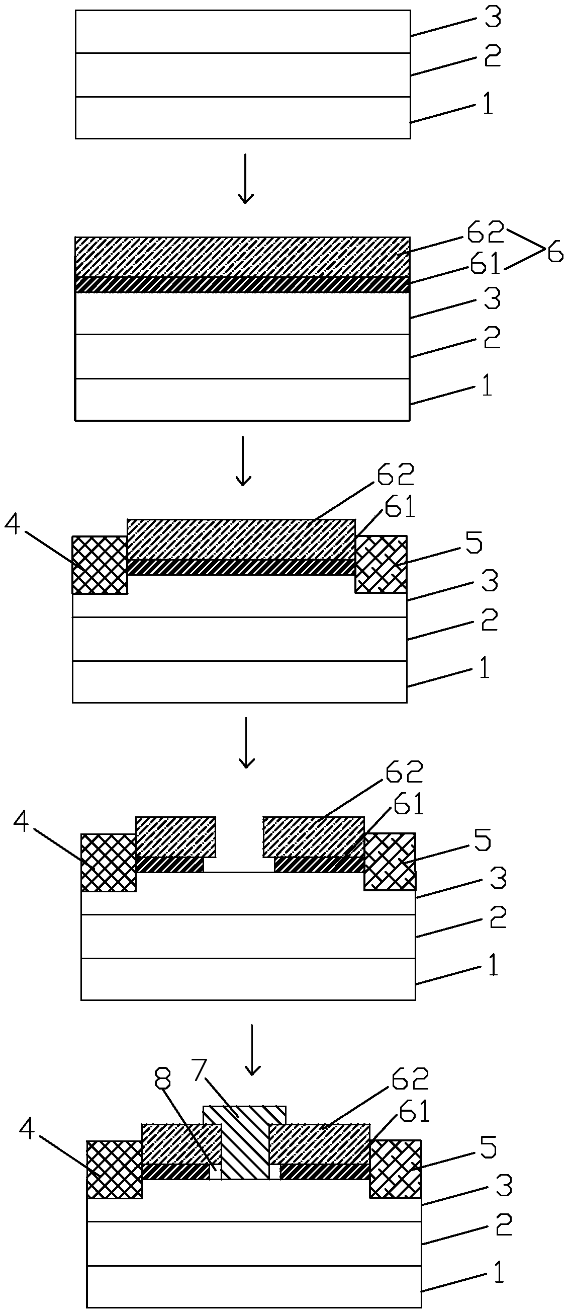
[0038] 1) With reference to Example 1.

[0039] 2) After cleaning, deposit SiOx medium on the surface of the barrier layer by PECVD method to form the lower dielectric layer, and then deposit AlO on the lower dielectric layer by ALD method x An upper dielectric layer is formed, and the lower dielectric layer and the upper dielectric layer form a composite passivation dielectric layer.

[0040] 3) using Cl-containing plasma to etch the upper dielectric layer, and then using F-based plasma to etch the lower dielectric layer, thereby forming a window on the composite passivation dielectric layer, and controlling the window width of the lower dielectric layer to be greater than that of the upper dielectric layer by controlling the etching time medium layer. The Al-based medium is etched with Cl-containing plasma, which has a relatively fast etching rate, and the F-based plasma is basically etched without moving; on...

Embodiment 3

[0044] The production method of this embodiment is as follows:

[0045] 1) With reference to Example 1.

[0046] 2) After cleaning, an Al-based dielectric is deposited on the surface of the barrier layer to form a lower dielectric layer, and then a Si-based dielectric is deposited on the lower dielectric layer to form an upper dielectric layer, and the lower dielectric layer and the upper dielectric layer form a composite passivation dielectric layer.

[0047] 3) Etching the upper dielectric layer with F-based plasma, and then wet-etching the lower dielectric layer with an alkaline solution to form a window on the composite passivation dielectric layer, and controlling the window width of the lower dielectric layer to be larger than the upper dielectric layer by controlling the etching time layer. The wet etching process has almost no etching effect on the Si-based dielectric.

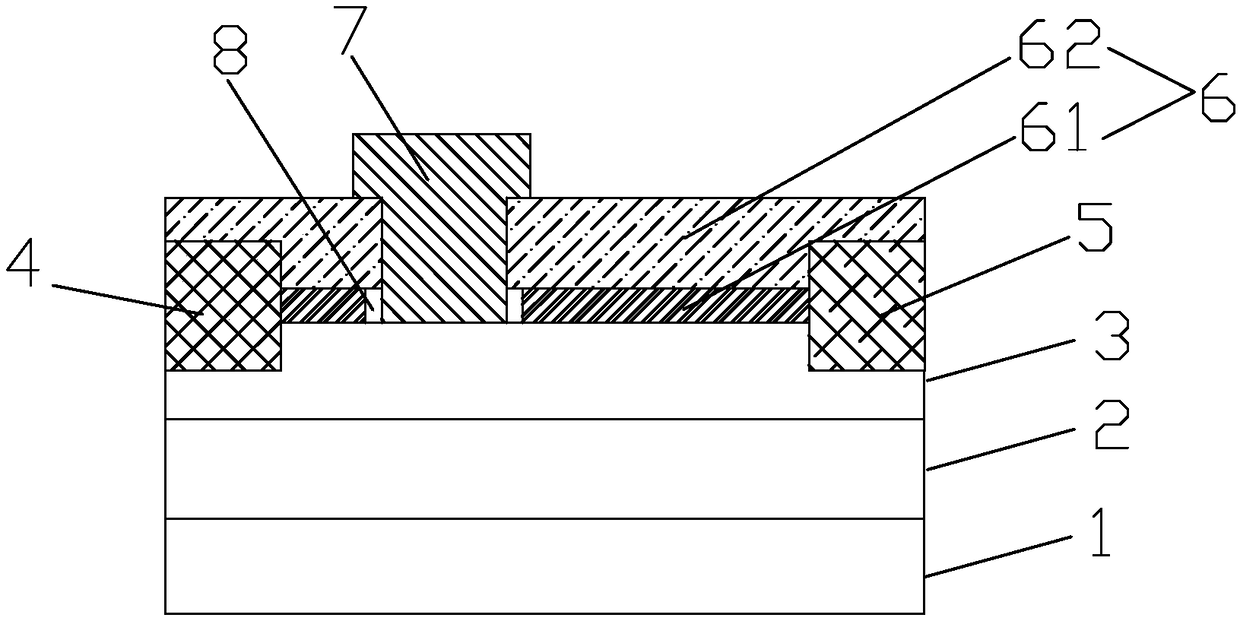
[0048] 4) Referring to Example 1, a gallium nitride transistor with a gap-type composite passivat...


PUM


Abstract

The invention discloses a gallium-nitride transistor employing a gap-type composite passivation medium and a manufacturing method. The composite passivation medium technology is employed, and the composite passivation medium at least comprises a lower dielectric layer and an upper dielectric layer, which are stacked. Moreover, the upper and lower dielectric layers have different etching characteristics. A specific etching method is employed for enabling the window width of the lower dielectric layer to be greater than the window width of the upper dielectric layer, so as to introduce a gap structure in a single passivation layer or multiple passivation layers making contact with a semiconductor and achieve the physical separation of a gate metal with a passivation medium/semiconductor interface, thereby cutting off an electric leakage channel on the surface of a device, and reducing the gate electric leakage on the surface of the device. Meanwhile, the good passivation effect can be maintained while the cutting of the electric leakage channel on the surface is achieved through the control of the width of the gap structure.

Description

technical field [0001] The invention relates to the technical field of semiconductors, in particular to a gallium nitride transistor with a gap-type compound passivation medium and a manufacturing method thereof. Background technique [0002] Gallium Nitride (GaN), as a representative of the third-generation wide bandgap semiconductor, has the advantages of large bandgap width, high electron mobility and high breakdown field strength. Since multi-component materials are more complex than single-component materials such as silicon, heterogeneous lattice growth mismatch, polarization effects, etc. have made the surface state problem a difficult problem that has not been systematically resolved from the early research stage to the present. The reasons include N vacancies, organic Factors such as the stop of the ordered lattice on the surface. These surface states are generally located in a relatively deep position in the forbidden band, appearing as a deep level trap. These d...

Claims


Application Information

Patent Timeline
Patent Type & Authority Applications(China)
IPC IPC(8): H01L21/335H01L29/778H01L29/06
CPCH01L29/0638H01L29/66462H01L29/7787
Inventor 刘胜厚周泽阳许若华蔡文必
Owner XIAMEN SANAN INTEGRATED CIRCUIT
Why Eureka
Try Eureka