

LED epitaxial wafer with quantum well barrier layer, growing method and LED structure
A technology of LED epitaxial wafer and quantum well layer, applied in electrical components, circuits, semiconductor devices, etc., can solve the problems of complex means, increase the concentration of quantum well holes, reduce stress, etc., to increase luminous efficiency, improve injection, Increase the effect of injection
- Summary
- Abstract
- Description
- Claims
- Application Information
AI Technical Summary
Problems solved by technology
Method used
Image

Examples
Embodiment 1
[0049] The present invention adopts Metal Organic Chemical Vapor Deposition (MOCVD, Metalorganic Chemical Vapor Deposition) growth, preferably, the sapphire of (0001) crystal orientation is selected as the substrate, high-purity H 2 or high purity N 2 or high purity H 2 and high purity N 2 The mixed gas is used as the carrier gas, and the metal-organic source and the nitrogen source are trimethylgallium (TMGa), trimethylindium (TMIn), triethylgallium (TEGa), trimethylaluminum (TMAl) and ammonia ( NH 3 ), the n-type dopant is silane (SiH 4 ), the p-type dopant is magnesium dicene (Cp 2 Mg).
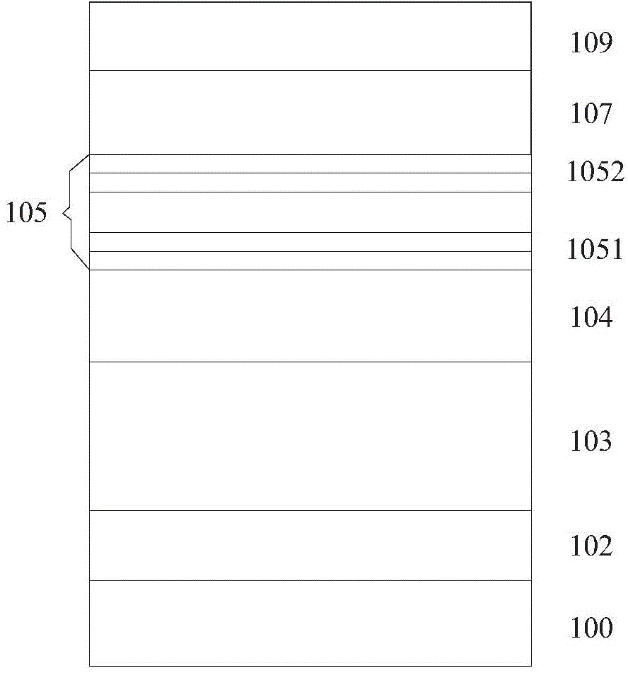
[0050] The method for growing an LED epitaxial wafer with a quantum well barrier layer includes the following growth steps in sequence:
[0051] a. Treat the sapphire substrate at high temperature for 5 minutes under a hydrogen atmosphere of 50L-60L;
[0052] b. Growing a low-temperature GaN buffer layer on a sapphire substrate;
[0053] c. Continue to grow the non-doped GaN layer;...
Embodiment 2
[0072] The growth method of the present embodiment is the same as the a, b, c, d, f, g, h growth steps of embodiment 1, step e:
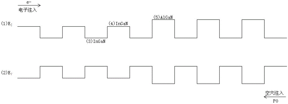
[0073] The pressure of the reaction chamber is maintained at 400mbar, the low temperature is 750°C, and NH 3 , TEGa, TMIn grow In-doped In with a thickness of 3.5nm x Ga (1-x) N layer (x=0.15~0.25), In doping concentration 1E+20~3E+20atom / cm 3 , heated up to 850°C and fed NH 3 , TEGa, TMIn grow In with a thickness of 15nm y Ga (1-y) N layer (y=0.05~0.10), In doping concentration 1E+18~2E+18atom / cm 3 ;In x Ga (1-x) N / In y Ga (1-y) The period number of the N quantum well layer is 5.
[0074] Next, the pressure of the reaction chamber is maintained at 400mbar, the low temperature is 700-750°C, and NH 3 , TEGa, TMIn grow In-doped In with a thickness of 3.5nm m Ga (1-m) N layer (m=0.15-0.25), In doping concentration 1E+20~3E+20atom / cm 3 , heated up to 850°C, fed NH 3 , TEGa, TMAl growth of Al with a thickness of 15nm n Ga (1-n) N layer (...
Embodiment 3
[0087] The growth method of the present embodiment is the same as the a, b, c, d, f, g, h growth steps of embodiment 1, step e:
[0088] The pressure of the reaction chamber is maintained at 300mbar, the low temperature is 750°C, and NH 3 , TEGa, TMIn grow In-doped In with a thickness of 2.8nm x Ga (1-x) N layer (x=0.15~0.25), In doping concentration 1E+20~3E+20atom / cm 3 , heated up to 850°C and fed NH 3 , TEGa, TMIn grow In with a thickness of 10nm y Ga (1-y) N layer (y=0.05~0.10), In doping concentration 1E+18~2E+18atom / cm 3 ;In x Ga (1-x) N / In y Ga (1-y) The period number of the N quantum well layer is 6.
[0089] Next, the pressure of the reaction chamber was maintained at 300mbar, the low temperature was 750°C, and NH 3 , TEGa, TMIn grow In-doped In with a thickness of 2.8nm m Ga (1-m) N layer (m=0.15-0.25), In doping concentration 1E+20~3E+20atom / cm 3 , heated up to 850°C, fed NH 3 , TEGa, TMAl grow Al with a thickness of 10-15nm n Ga (1-n) N layer (n=0....
PUM
 Abstract
Description
Claims
Application Information