

Wave aberration measuring device and measuring method of optical system
An optical system and measurement device technology, applied in the field of optical measurement, can solve problems such as high-precision detection of wave aberrations in optical systems that are difficult to achieve, reduce the influence of stray light, improve energy utilization, and improve measurement speed and accuracy. Effect
- Summary
- Abstract
- Description
- Claims
- Application Information
AI Technical Summary
Problems solved by technology
Method used
Image

Examples
no. 1 example
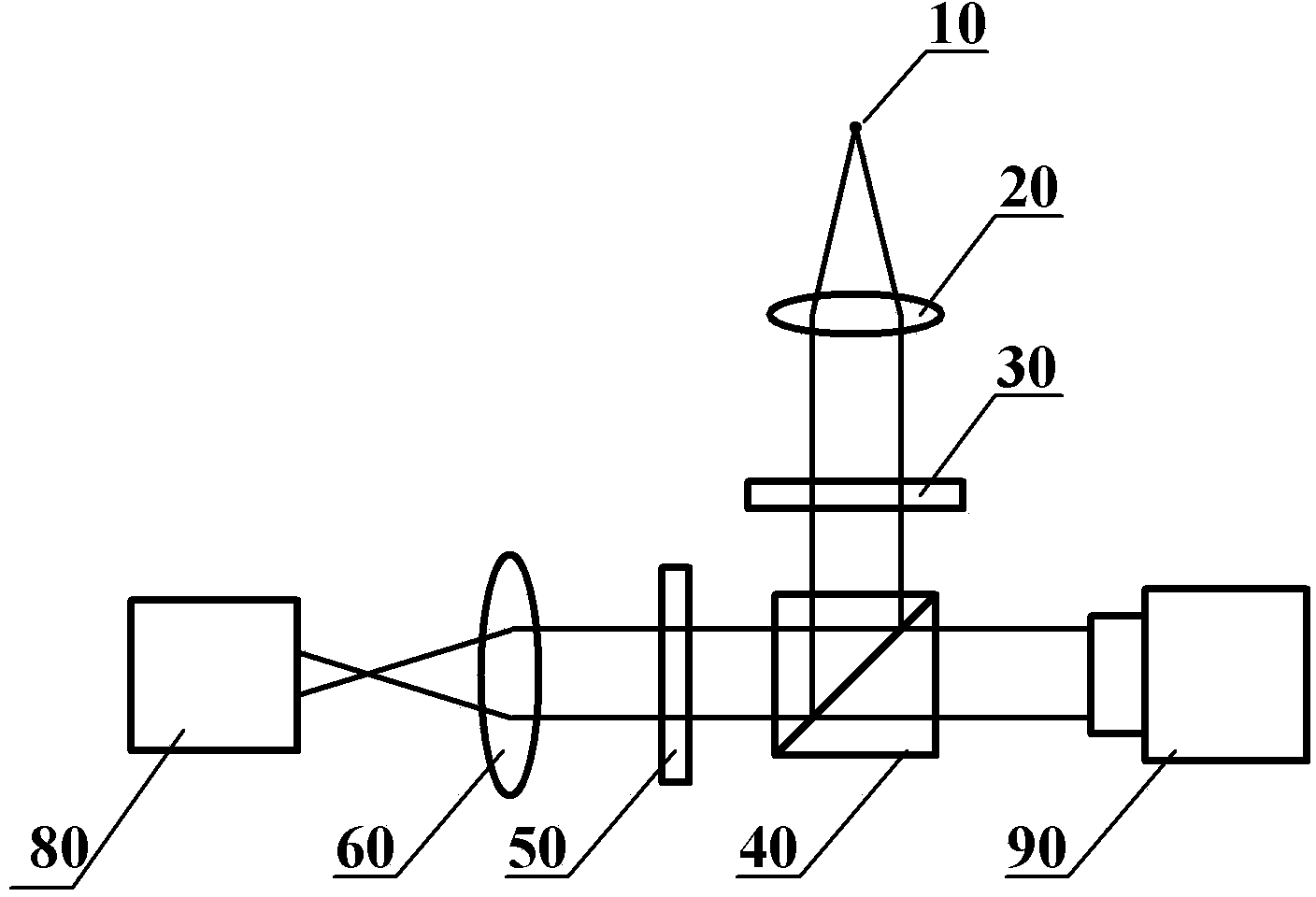
[0039] Figure 1A It is a structural diagram of the first embodiment of the optical system wave aberration measuring device of the present invention, and this embodiment is a measuring device for measuring wave aberration of a finite or infinite conjugate optical system. like Figure 1A As shown, the measurement device includes a linearly polarized spherical wave point source 10, a first collimating mirror 20, a 1 / 2 wave plate 30, a polarization beam splitter prism 40, a 1 / 4 wave plate 50, a second collimating mirror 60, and a reflection device 80 and the Shaker-Hartmann wavefront sensor 90.
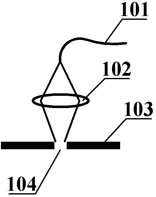
[0040] In this embodiment, the microhole can be used as the illumination system when the linearly polarized spherical wave point source is used. Figure 1B shows its specific structure, such as Figure 1B As shown, the linearly polarized spherical wave point source includes a single-mode linear polarization maintaining optical fiber 101 for transmitting linearly polarized light, an imag...
no. 2 example
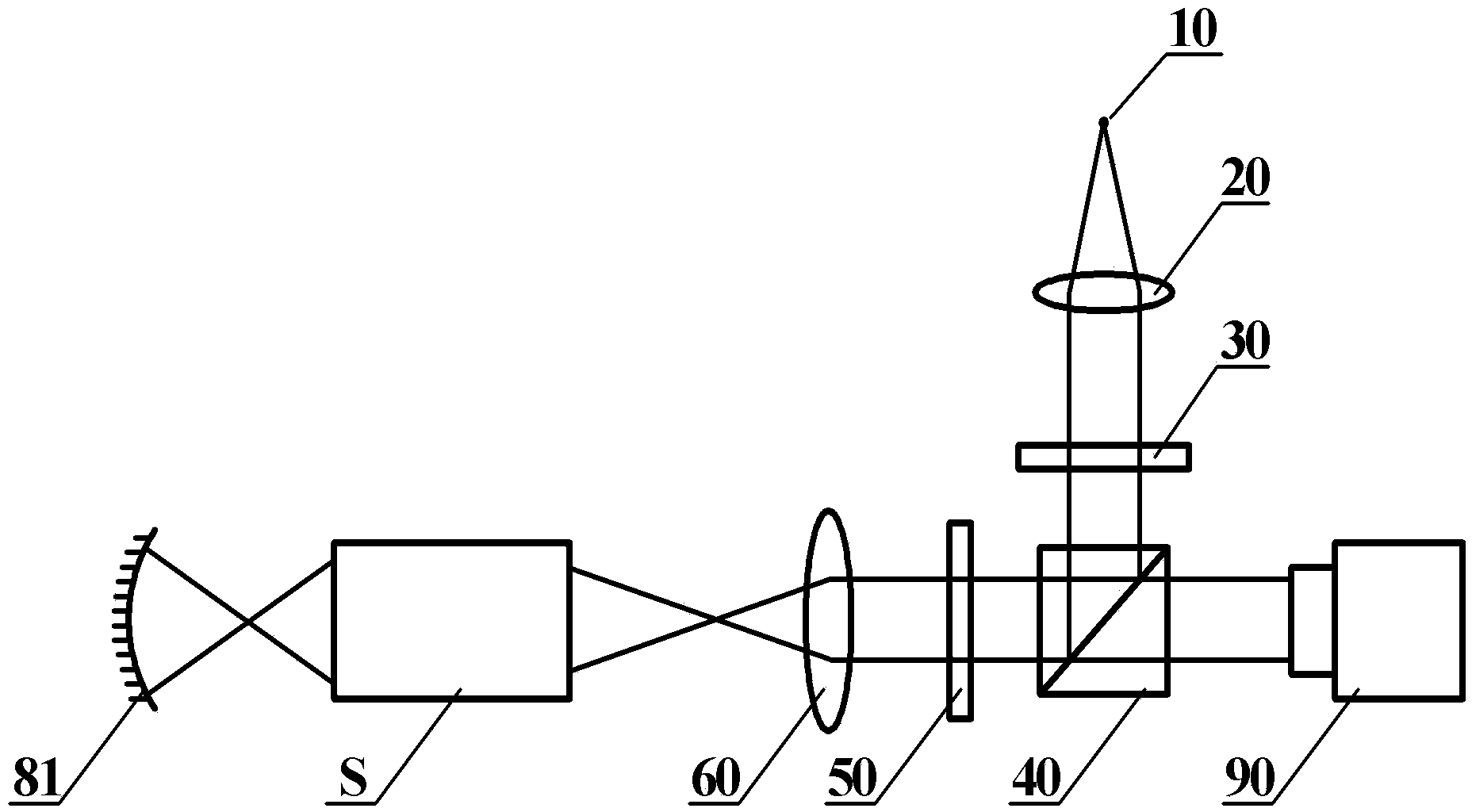
[0054] Figure 4 It is a structural diagram of the second embodiment of the optical system wave aberration measuring device of the present invention, which is a measuring device for measuring wave aberration of an infinite conjugate optical system or a transmitted plane wave optical system. like Figure 4 shown, compared to Figure 1A In the first embodiment shown, the second collimating lens 60 is not included in the measuring device. That is to say, in the measuring device of the second embodiment, the circularly polarized plane wave emitted by the 1 / 4 wave plate is directly emitted to the reflecting device 80 , and returned after being reflected by the reflecting device 80 .
[0055] Figure 5A and Figure 5B is to use Figure 4 The schematic diagram of the optical system wave aberration measuring device when measuring the wave aberration of the conjugate optical system at infinity is shown, wherein Figure 5A Shown is the overall wave aberration used to measure the op...
PUM
 Abstract
Description
Claims
Application Information