

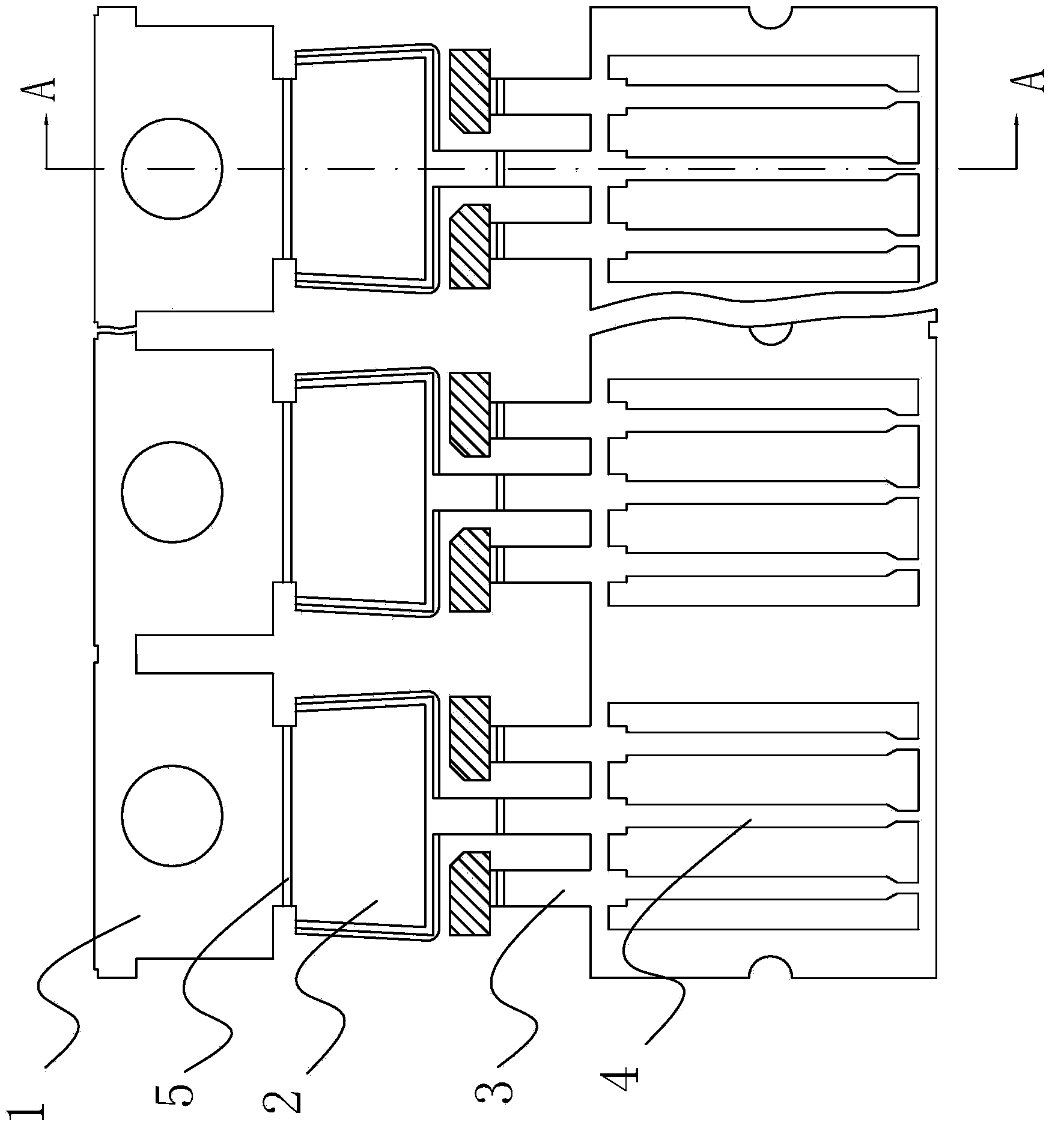
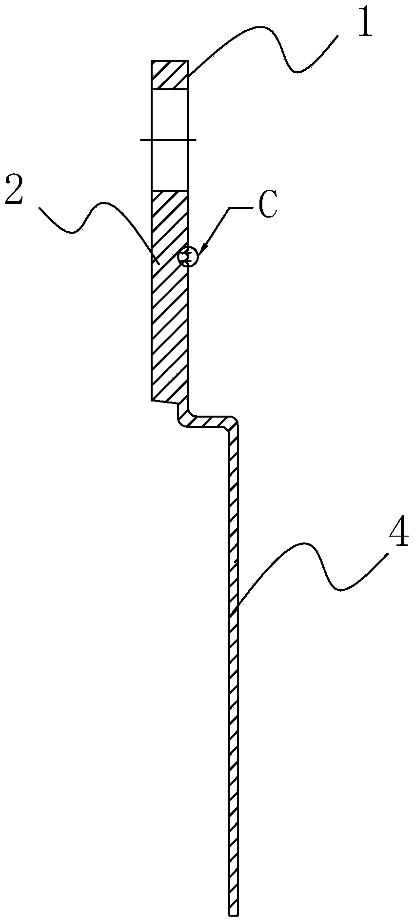
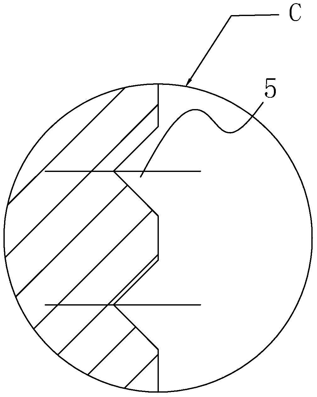
Lead wire frame copper plating method, lead wire frame, lead wire frame row
A lead frame and copper plating technology is applied in the field of lead frames, lead frames that are easier to manufacture and lead frame rows, which can solve the problems of high cost and complex structure, and achieve the effect of saving cost and being beneficial to miniaturization.
- Summary
- Abstract
- Description
- Claims
- Application Information
AI Technical Summary
Problems solved by technology
Method used
Image

Examples
Embodiment 1
[0036] The lead frame aluminum alloy base is made of the following elements by weight percentage:
[0037] Magnesium: 0.4%, silicon: 0.02%, copper: 0.5%, manganese: 0.02%, chromium: 0.1%, zirconium: 0.05%, and the balance is aluminum and unavoidable impurities.
[0038] Silicon element can strengthen the corrosion resistance of aluminum alloy, improve yield strength and elasticity, but excessive silicon element will reduce the welding performance of alloy materials.
[0039] Manganese can promote grain growth and improve the rigidity of the alloy, but excessive manganese will reduce the corrosion resistance of the alloy.
[0040] Chromium can improve the strength, hardness and toughness of the alloy, so its content is high, but the combination of chromium and aluminum will reduce the resistance of the alloy, which is not conducive to the electrical conductivity of the lead frame.
[0041] The zirconium element improves the thermal stability of the alloy while reducing the bri...
Embodiment 2
[0058] The lead frame aluminum alloy base is made of the following elements by weight percentage:
[0059] Magnesium: 1.0%, silicon: 0.5%, copper: 0.2%, manganese: 0.04%, chromium: 0.3%, zirconium: 0.1%, and the balance is aluminum and unavoidable impurities.
[0060] Copper-plating the aluminum alloy lead frame substrate made according to the following steps:
[0061] Degreasing and degreasing, potion composition and content:
[0062] Sodium hydroxide: 38%, sodium metasilicate: 35%, degreasing agent: 40g / L, degrease and degrease at 50°C-70°C;
[0063] One-time zinc dipping: Put the degreased aluminum alloy substrate into a mixed solution with a concentration of zinc ions of 40g / L, a concentration of iron oxide of 65g / L, and a concentration of sodium hydroxide of 230g / L for zinc dipping, and the zinc dipping temperature is 57 °C; then wash with water at a temperature of 50 °C;
[0064] One-time pickling: put the aluminum alloy substrate after one-time zinc dipping into the ...
Embodiment 3
[0075] The lead frame aluminum alloy base is made of the following elements by weight percentage:
[0076] Magnesium: 1.5%, silicon: 0.8%, copper: 0.2%, manganese: 0.2%, chromium: 0.3%, zirconium: 0.25%, and the balance is aluminum and unavoidable impurities.
[0077] Copper-plating the aluminum alloy lead frame substrate made according to the following steps:
[0078] Degreasing and degreasing, potion composition and content:
[0079] Sodium hydroxide: 45%, sodium metasilicate: 40%, degreasing agent: 40g / L, degrease and degrease at 50°C-70°C;
[0080] One-time zinc dipping: Put the degreased aluminum alloy substrate into a mixed solution with a zinc ion concentration of 45g / L, an iron oxide concentration of 70g / L, and a sodium hydroxide concentration of 250g / L for zinc dipping, and the zinc dipping temperature is 60 °C; then wash with water at a temperature of 50 °C;
[0081] One-time pickling: put the aluminum alloy substrate after one-time galvanizing into a nitric acid ...
PUM
| Property | Measurement | Unit |
|---|---|---|
| thickness | aaaaa | aaaaa |
| thickness | aaaaa | aaaaa |
| thickness | aaaaa | aaaaa |
Abstract
Description
Claims
Application Information