Organic semiconductor material, preparation method thereof and electroluminescent device
A technology of electroluminescent devices and organic semiconductors, applied in the fields of electroluminescent devices, preparation, and organic semiconductor materials, can solve the problems of lack of carrier transport performance, low glass transition temperature, high triplet energy level, etc., and achieve It is beneficial to the balance of carrier transport, high triplet energy level, and the effect of simple and easy synthesis method
- Summary
- Abstract
- Description
- Claims
- Application Information
AI Technical Summary
Problems solved by technology
Method used
Image

Examples
preparation example Construction
[0025] The invention provides a kind of preparation method of organic semiconductor material, comprises the steps:
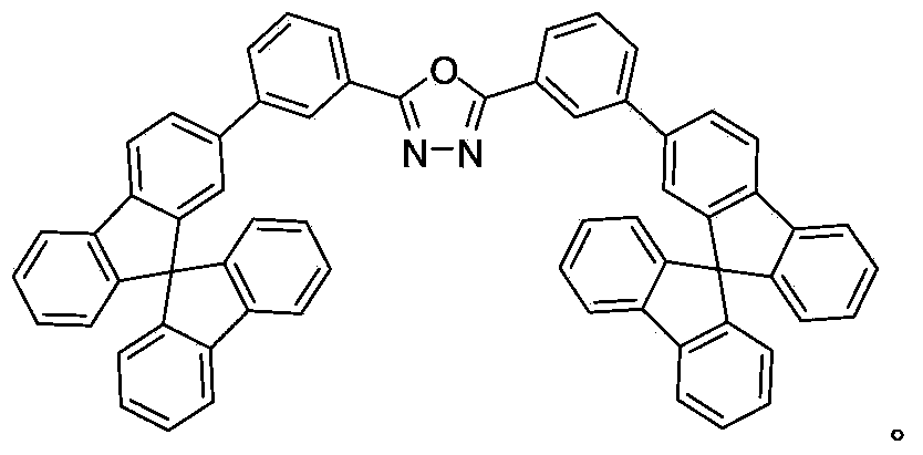
[0026] Provides compound A: and compound B: Under an inert atmosphere, compound A and compound B are added into an organic solvent containing a catalyst and an alkali solution at a molar ratio of 1:2 to 2.4, and the Suzuki coupling reaction is carried out at 70 to 130°C for 12 to 48 hours, and the reaction is stopped to obtain an organic The chemical formula of a semiconductor material is as follows:
[0027]
[0028] The preparation method of the organic semiconductor material further includes a post-processing step, and the post-processing step is specifically: extracting the organic semiconductor material obtained by stopping the reaction with dichloromethane, combining the organic phases, drying them with anhydrous magnesium sulfate, and using petroleum A mixed solvent of ether and ethyl acetate was used as eluent, separated and purified through a sil...
Embodiment 1
[0041] 2-(3-(9,9'-spirobifluoren-2-yl)phenyl)-5-(3-(9,9'-spirobifluoren-7-yl)phenyl)-1,3, The preparation process of 4-oxadiazole preparation steps are as follows:
[0042]
[0043]Under argon protection, 2,5-bis(3-bromophenyl)-1,3,4-oxadiazole (76 mg, 0.2 mmol), 2-pinacol borate-9,9-spiro Difluorene (177mg, 0.4mmol) was added to a flask containing 10ml of toluene solvent, and after fully dissolving, potassium carbonate (2mL, 2mol / L) solution was added to the flask, vacuumed to remove oxygen and filled with argon, and then added bis Triphenylphosphinepalladium dichloride (5.6mg, 0.008mmol); the flask was heated to 100°C for Suzuki coupling reaction for 24h. The reaction was stopped and cooled to room temperature, extracted three times with dichloromethane, the organic phases were combined, dried over anhydrous magnesium sulfate and then spin-dried to obtain the 2-(3-(9,9'-spirobifluoren-2-yl)phenyl )-5-(3-(9,9'-spirobifluoren-7-yl)phenyl)-1,3,4-oxadiazole organic semicond...
Embodiment 2
[0048] 2-(3-(9,9'-spirobifluoren-2-yl)phenyl)-5-(3-(9,9'-spirobifluoren-7-yl)phenyl)-1,3, The preparation process of 4-oxadiazole preparation steps are as follows:
[0049]
[0050] Under the protection of mixed gas of nitrogen and argon, 2,5-bis(3-bromophenyl)-1,3,4-oxadiazole (76mg, 0.2mmol), 2-pinacol borate-9 , 9-spirobifluorene (292mg, 0.66mmol) and 15mL tetrahydrofuran were added into a 50mL two-necked bottle, fully dissolved, and then a mixture of nitrogen and argon was introduced to exhaust the air for about 20 minutes, and then tetrakistriphenylphosphine palladium ( 4mg, 0.003mmol) into it, fully dissolved and then added sodium bicarbonate (3mL, 2mol / L) solution. Then, the mixed gas of nitrogen and argon was exhausted for about 10 minutes, and the two-neck flask was added to 70°C for Suzuki coupling reaction for 48 hours. The reaction was stopped and cooled to room temperature, extracted three times with dichloromethane, the organic phases were combined, dried ov...
PUM
 Abstract
Description
Claims
Application Information
 - R&D
- Intellectual Property
- Life Sciences
- Materials
- Tech Scout
- Unparalleled Data Quality
- Higher Quality Content
- 60% Fewer Hallucinations
Browse by: Latest US Patents, China's latest patents, Technical Efficacy Thesaurus, Application Domain, Technology Topic, Popular Technical Reports.
© 2025 PatSnap. All rights reserved.Legal|Privacy policy|Modern Slavery Act Transparency Statement|Sitemap|About US| Contact US: help@patsnap.com