A method for preparing a highly sensitive surface-enhanced Raman scattering substrate

A surface-enhanced Raman and high-sensitivity technology, applied in the field of analysis and detection, can solve problems that have not caused researchers, and achieve the effect of improving the probability of being located on a hot spot and high detection sensitivity

Inactive Publication Date: 2016-08-24
JILIN UNIV
View PDF7 Cites 0 Cited by
  • Summary
  • Abstract
  • Description
  • Claims
  • Application Information

AI Technical Summary

Problems solved by technology

However, this phenomenon has not attracted widespread attention from researchers.

Method used


Image

  • A method for preparing a highly sensitive surface-enhanced Raman scattering substrate
  • A method for preparing a highly sensitive surface-enhanced Raman scattering substrate
  • A method for preparing a highly sensitive surface-enhanced Raman scattering substrate

Examples


Embodiment 1

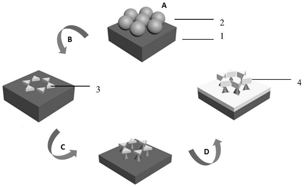
[0035] Arranging colloidal balls with a diameter of 360nm on the surface of a silicon chip to form a single-layer colloidal ball array: (1) adding an equal volume of ethanol solution to an aqueous solution of polystyrene colloidal balls with a diameter of 360nm and a concentration of 10wt%, and ultrasonicating for 2h; ( 2) Cleaning the silicon wafers: Sonicate the silicon wafers in acetone, chloroform, ethanol and water for 5 minutes in sequence, and then wash the silicon wafers with a mixed solution of concentrated sulfuric acid (98wt%) and hydrogen peroxide (30wt%) (volume ratio 3:1) Wash at 80°C for 1 h, and finally rinse with deionized water and blow dry with nitrogen; (3) Assembly and transfer of polystyrene colloidal sphere monolayer film: first, add 200 mL of deionized water to a clean watch glass, and Add 20 μL of surfactant (1wt% sodium lauryl sulfate solution); secondly, place the volleyball silicon chip against the edge of the watch glass, so that it is partially imm...

Embodiment 2

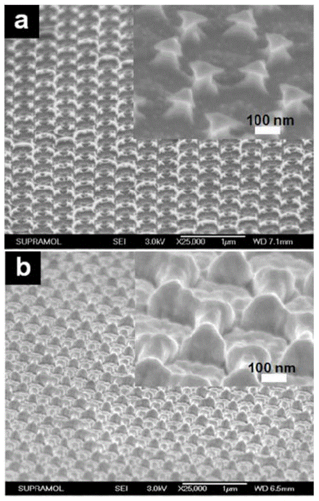
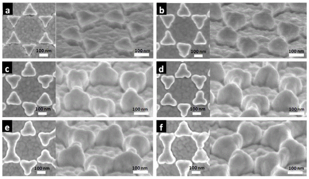
[0038] The SERS test was carried out for the suspended nano-antenna with the thickness of the silver film ranging from 20 to 180nm. Figure 4 a shows the SERS spectra of suspended nanoantenna arrays with different silver film thicknesses, and the scale bar in the figure represents 20000 cps. The strongest SERS signal is the suspended nanoantenna structure covered with 95nm silver film. Figure 4 b shows the peak at 1091cm -1The relationship between the SERS intensity and the thickness of the silver film. As the silver film thickness increases from 20nm to 95nm, the SERS intensity increases continuously. However, when the silver film thickness increased from 120nm to 180nm, the SERS intensity decreased continuously.

Embodiment 3

[0040] The near-field distribution on the surface of suspended nanoantennas with different silver film thicknesses was simulated by finite time-domain difference method (Lumerical FDTD Solutions software). In order to make the model closer to the actual sample, each vertex of the triangle is truncated. According to geometrical calculations, for a sphere with a period of 360nm, the side length of each Ag triangle is 177.68nm, and the truncated side length is 10nm. At this time, the gap spacing is 20nm. Similarly, the Au triangle has a side length of 130nm and a truncated side length of 5nm. For the sake of simplicity, the silicon column is replaced by a cylinder with a diameter of 40nm and a height of 80nm. There is an air cavity with the same shape as the silver triangle directly below each suspended triangle, which is located in the silver film and has the same height as the thickness of the evaporated silver film. The refractive indices of Si, Ag, and Au are from the Palik...


PUM

PropertyMeasurementUnit
diameteraaaaaaaaaa
lengthaaaaaaaaaa
thicknessaaaaaaaaaa

Abstract

A method for preparing a highly sensitive surface-enhanced Raman scattering substrate belongs to the technical field of analysis and detection. Specifically, an array of suspended nanoantenna structures is constructed on a silicon substrate. The vibration mode of the metal nanostructure can be controlled by the thickness of the evaporated silver. With the increase of the thickness of the evaporated silver film, the shape and vibration mode of the suspended nanoantenna can be changed. Mutation occurs. This mutation not only increases the strength of the hotspot, but also shifts the location of the hotspot from the bottom to the top of the nanoantenna. On this basis, with the help of the molecular confinement effect caused by the hydrophobicity of the silver surface, the possibility of hot spots contacting the molecules to be detected is increased, and the detection sensitivity of the SERS substrate is improved. The optimized suspended nanoantenna array achieves higher SERS sensitivity, and its maximum SERS enhancement factor is 9.8×10 9 , the minimum detection concentration is 10 ‑12 mol / L.

Description

technical field [0001] The invention belongs to the technical field of analysis and detection, and in particular relates to a method for preparing a high-sensitivity surface-enhanced Raman scattering (SERS) substrate. Background technique [0002] Optical nanoantenna is a metal nanostructure that can effectively capture electromagnetic waves at optical frequencies to achieve nanoscale electromagnetic field energy concentration and confinement. Optical nanoantennas usually use slits with very small spacing or tip structures with very small curvature radii to generate extremely small and extremely strong localized electric fields. Such sites are called "hot spots". Gold and silver nano bow tie structures (Nano Lett.2004,4,957; J.Phys.Chem.Lett.2013,4,496; Appl.Phys.Lett.2013,103,041903; Nano Lett.2012,12,796) as a typical The nanoantennas of the present invention generate hotspots by virtue of the tip-to-tip arrangement of two nanotriangular triangles that are very close to e...

Claims


Application Information

Patent Timeline
Patent Type & Authority Patents(China)
IPC IPC(8): G01N21/65
Inventor 吕男马任平封雷徐大任王燕东刘凌霄
Owner JILIN UNIV
Why Eureka
Try Eureka