LED growth method with n-type layer coarsening

A growth method, N-type technology, applied in the direction of electrical components, circuits, semiconductor devices, etc., to achieve the effect of improving light extraction efficiency, realizing industrialization, and simple and easy roughening method

Active Publication Date: 2017-09-29
EPITOP PHOTOELECTRIC TECH
View PDF5 Cites 0 Cited by
  • Summary
  • Abstract
  • Description
  • Claims
  • Application Information

AI Technical Summary

Problems solved by technology

[0005] Although the use of these technologies has enabled GaN-LEDs to achieve significant optoelectronic performance improvements in recent years, in the existing LED growth methods for roughening the N-type layer, not only secondary growth is required, but also the modification of the P-type layer is required.

Method used


Image

  • LED growth method with n-type layer coarsening
  • LED growth method with n-type layer coarsening
  • LED growth method with n-type layer coarsening

Examples


Embodiment 1

[0050] GaN blue LED with roughened N-type layer

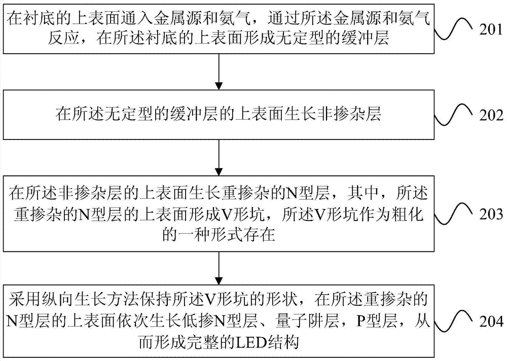
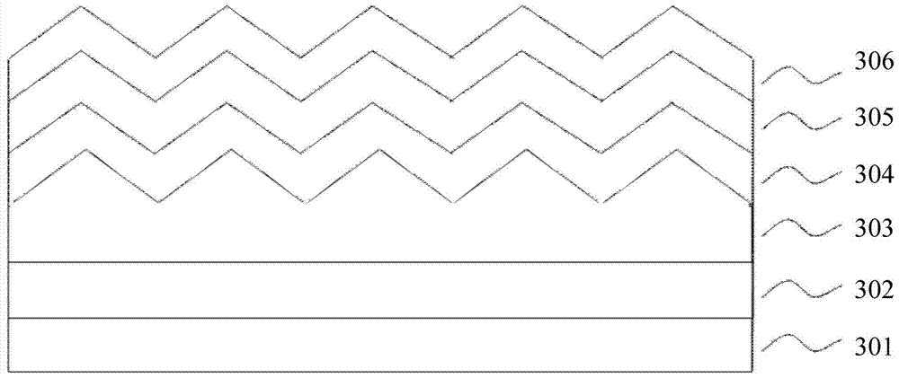
[0051] 1. On the Veeco MOCVD K465I machine, use a patterned sapphire substrate. When the surface temperature of the substrate material 301 rises to about 530°C, keep the growth pressure at 500 Torr. Pass trimethylgallium (60ml / min) and ammonia gas (NH 3 )50l / min for 3 minutes, trimethylgallium and NH 3 At this temperature, it decomposes and reacts chemically to form an amorphous buffer layer with a thickness of 20nm.

[0052] 2. Increase the temperature of the reaction chamber to 1000°C. At this time, the buffer layer undergoes decomposition and polymerization to form uniformly distributed nucleation islands. Then, on this basis, the pressure is maintained at 500 Torr, and trimethylgallium (200ml / min) and NH 3 50l / min reaction for 30 minutes. This growth process can make the crystal nucleus islands grow and merge, without doping any impurities to form the undoped GaN layer 302 . The thickness of this layer is approximately...

Embodiment 2

[0059] GaN green LED with roughened N-type layer

[0060] 1. On the Veeco MOCVD K465I machine, use a patterned sapphire substrate. When the surface temperature of the substrate material 301 rises to about 530°C, keep the growth pressure at 500 Torr. Pass trimethylgallium (60ml / min) and ammonia gas (NH 3 )50l / min for 3 minutes, trimethylgallium and NH 3 At this temperature, it decomposes and reacts chemically to form an amorphous buffer layer with a thickness of 20nm.

[0061] 2. Increase the temperature of the reaction chamber to 1000°C. At this time, the buffer layer undergoes decomposition and polymerization to form uniformly distributed nucleation islands. Then, on this basis, the pressure is maintained at 500 Torr, and trimethylgallium (200ml / min) and NH 3 50l / min reaction for 30 minutes. This growth process can make the crystal nucleus islands grow and merge, without doping any impurities to form the undoped GaN layer 302 . The thickness of this layer is approximatel...


PUM


Abstract

The embodiment of the invention provides an LED growth method for N-type layer coarsening. The method includes the steps that a metal source and ammonia are fed into the upper surface of a substrate, the metal source reacts with the ammonia, and consequently an amorphous buffer layer is formed on the upper surface of the substrate; a non-doping layer grows on the upper surface of the amorphous buffer layer; a high doping N-type layer grows on the upper surface of the non-doping layer, wherein V-shaped pits are formed in the upper surface of the high doping N-type layer and exist in a form of coarsening. A longitudinal growth pattern is adopted to maintain the shape of the V-shaped pits, a low doping N-type layer, a quantum well layer and a P-type layer grow on the upper surface of the high doping N-type layer in sequence, and therefore a complete LED structure is formed. Secondary growth is not needed, the P-type layer does not need to be transformed, and the chip manufacturing process cannot be excessively influenced.

Description

technical field [0001] Embodiments of the present invention relate to semiconductor manufacturing technology, and in particular to an LED growth method for roughening an N-type layer. Background technique [0002] The wide bandgap material represented by gallium nitride (GaN) is the third-generation semiconductor material after silicon (Si) and gallium arsenide (GaAs). GaN can be used to make light-emitting diodes, lasers, detectors, high Electronic devices such as high-frequency high-power transistors. [0003] At present, the production of light-emitting diodes (Light Emitting Diode, referred to as LED) with GaN materials is relatively mature, and its application is becoming more and more extensive, especially in many fields such as landscape lighting, street lighting, backlight, and indoor lighting. Well behaved. However, as LEDs become more and more widely used, the problems exposed by LEDs are becoming more and more prominent: for applications in the lighting field, t...

Claims


Application Information

Patent Timeline
Patent Type & Authority Patents(China)
IPC IPC(8): H01L33/00
CPCH01L33/007H01L33/22
Inventor 黄小辉马刚蔡武周德保康建梁旭东
Owner EPITOP PHOTOELECTRIC TECH
Why Eureka
Try Eureka